My Pi Description

My Experiences With the Raspberry Pi -- Tracking My Learning -- My Pi Projects

Tuesday, December 16, 2014

Jig To Load a Bootloader and Upload Sketches To ATmega328P

Note: I only write about what I know. Although there are many Arduinos and Arduino type products, I only have experience with the Arduino Uno Rev3. Likewise, the only Atmel microcontroller I know is the ATmega328P.

A Little Background (well not so little)

I have Atmel ATmega328P microcontrollers on two devices: An Arduino Uno (Rev 3), and a Gertboard. The Gertboard connects to, and is programmed by, my Raspberry Pi. In both cases the microcontroller is in a socket, so is removable. I have developed applications for both where I needed to remove the ATmega328P and install it in another device. I use the Arduino IDE system to develop sketches on both the Arduino and the Gertboard/Raspberry Pi. There is more on the Gertboard at the end of this post.
I developed a camera remote control using the Gertboard and removed the programmed ATmega chip and installed it on a circuit board. The circuit board, a 434MHz transmitter, and a motion detector were mounted in a box. I reported on that project in this blog entry.
I am completing a project that uses both the Arduino and the Gertboard/Raspberry Pi. In this case, it is the sketch developed on the Arduino that must run on an ATmega328P that is removed from the Arduino. This project, that I will report on later, requires the ability to communicate with the ATmega328P once it is installed in my mobile device.
Both projects required me to program a new ATmega328P IC. However, you can not just insert a new chip on the Arduino or Gertboard and upload sketches to it. Out of the box, the microcontroller will not use the external 16MHz crystal of the Arduino or the 12MHz resonator of the Gertboard. It will use its internal 8MHz RC oscillator frequency reference and then divide that frequency by 8. The resulting clock frequency will be 1MHz.
In order to change the clock source, you must change the logic level of a couple of "fuse" bits. I use "" around the word fuse, because the term is actually a carryover from the time when ICs, like microcontrollers, had actual fuses. Each fuse would control the logic level of one bit. If the fuse was blown, the bit would be a 0, if not blown it would be a 1. You could always change a 1 to a 0, by blowing the fuse, but you had no way to change a 0 to a 1. If you wanted a 1, but programmed a 0, in error, you had to replace the chip. That is not the case today.
Now, "fuse" bits can be changed from 1 to 0 and 0 to 1 anytime. The ATmega328P has three, eight bit bytes of these "fuse" bits. They control different functions and leave the factory in a default configuration. In addition, there is a byte (8 bits) of lock bits. More on these later. To setup a new ATmega328P for the Gertboard, you run a program on the Raspberry Pi called avrsetup. All this program does is to use avrdude to set the lock bits and the fuse bits. It leaves all bits not concerned with the clock frequency to their default settings. The four bits that select the clock source are changed from "Calibrated RC Internal Oscillator" to "Full Swing Crystal Oscillator". And, the divide by 8 function is turned off. Avrdude is like an operating system for the Atmel microcontrollers. All programming of the microcontrollers are done through avrdude even if you use the Arduino IDE.
For the Gertboard/Raspberry Pi, setting those fuse bits is all you have to do to use a new ATmetga328P. That is not the case with the Arduino. A new ATmega328P for the Arduino needs those same fuse bit changes and needs one more thing: a bootloader installed. What is a bootloader, and why doesn't the Gertboard need one?
When you upload a sketch to the flash memory of the ATmega328P, there are two direct ways. One is to use a parallel configuration, which I will not mention further (just going to forget it exists). The other is to use the chip's SPI (Serial Peripheral Interface) bus. This synchronous, serial, bus consists of four lines: SCK (Serial Clock), SS (Slave Select), MOSI (Master Out Slave In), and MISO (Master In Slave Out). I upload sketches to the Gertboard via the SPI bus. The Raspberry Pi is the Master, the ATmega328P on the Gertboard is the Slave. Since the direct programming method is employed, no bootloader is necessary.
Atmel, in their wisdom, realized that not everyone would like to use the SPI bus, but would wish to use the more universal serial bus (or something else). The serial bus interface has several names such as RS232 and UART. It consists of several signals: TX (transmitted data) and RX (received data). The TX of the one device is connected to the RX of the other device, and RX of the first device is connected to TX of the second device. There are more signals, but, typically, they are not used. However, a signal, DTR (data terminal ready), for example, may be used to reset the ATmega328P. Once the ATmega328P is reset, it will start running any sketch loaded in flash from its beginning.
Atmel provided an area of flash memory for the user to install code allowing the rest of the flash memory to be uploaded via the serial bus. This code is the bootloader. For the ATmega328P, it can take up as much as 2 Kbytes of the 32 Kbytes of flash memory. The flash memory, not reserved for the bootloader, is the Application memory. Once the bootloader is loaded, it can load a new sketch into the Application memory via the RX and TX connections of the serial bus.
So, how do you get the bootloader loaded in a new ATmega328P? It requires hardware and software. Since a new ATmega328P has no bootloader, the bootloader must be installed from the SPI bus - the direct, primary, interface to the chip. That means you need an in-circuit programmer. There are inexpensive, commercial, units available like the USBtinyISP. They have USB on one end and the four SPI connections on the other end (SCK, SS, MOSI, and MISO), plus power and ground. They have a 6 pin ribbon cable and connector that plugs into your target device that contains the microcontroller chip you want to access. There is a standard 6 pin SPI configuration that receives the ribbon cable connector. My Arduino Uno has two of these 6 pin connectors, one for the ATmega16U2 and the other for the ATmega328P. You can install a new ATmega328P on your Arduino Uno and connect a programmer to it to upload the bootloader. But, I don't do that.
I have no experience with the aforementioned programmers so I will not discuss them. There is another programmer that works really well - and I have experience with that one. This programmer is the Arduino itself. You can't use it to load a bootloader on its own ATmega328P, but it can be used to install a bootloader on another Arduino's ATmega328P. However, I do a variation of that. I use the Arduino Uno to install the bootloader on an ATmega328P that is on a jig I made. This is the jig that is the subject of this blog post.
Now we need some software. There are two pieces of this. One piece is the bootloader itself. The Arduino IDE package has copies of the bootloaders. There are different bootloaders for the different ATmega devices and the different Arduinos. The other piece of software is the software to load the bootloader. This software is a sketch running on my Arduino Uno that is used as a programmer. This software must do several things. I have not studied this software to know how it works, but from my knowledge of the ATmega328P, I know it must do the following:
  • Program the fuse bits to select the clock source to "Full Swing Crystal Oscillator" and turn off the clock divide by 8.
  • Set the Lock bits to allow programming of the bootloader in the Boot Flash Section
  • Set the fuse bits to the amount of flash memory devoted to the Boot Flash Section (up to 2 KBytes)
  • Upload the bootloader program to the Boot Flash Section
  • Set the lock bits so the Boot Flash Section can no longer be written to, protecting it from being overwritten.
There is one last point to consider before moving on to the details of my programming jig. Could there be an Arduino that programs the microcontroller directly over the SPI bus? Certainly. There are ICs that convert USB to SPI. That would eliminate the bootloader. We are forgetting one thing though: How do you communicate with a sketch? For example, a sketch that requires you to answer some questions before proceeding. The answer is the Serial Monitor. Access to the Serial Monitor is via the same interface the Arduino uses to upload sketchs - the same TX and RX connections to the ATmega328P.
For the Gertboard, the Serial Monitor button exists on the Arduino IDE running on the Raspberry Pi. However, it does not work. A separate connection to the ATmega328P's UART must be made. Consequently, the Raspberry Pi/Gertboard requires six signal connections: SCK, MOSI, MISO, SS, and TX and RX. The Arduino UNO only has two ATmega328P signal connections: TX and RX. For the Gertboard, I have to open a separate terminal window and run a terminal program to communicate with a running sketch. All-in-all, the loss of a little flash memory to the bootloader seems worthwhile.

An ATmega328P Programming Jig

The following is the schematics and board layout diagram for my jig:
Schematics For ATmega328P Programmer
Here is the layout of the board with components and wiring:
Board Layout For The ATmega328P Programmer
Looking at the board layout, the ATmega328P sits in a 28 pin ZIF socket (all that green in the diagram). This allows an IC to be quickly inserted and removed. Check out the product page from Sparkfun.
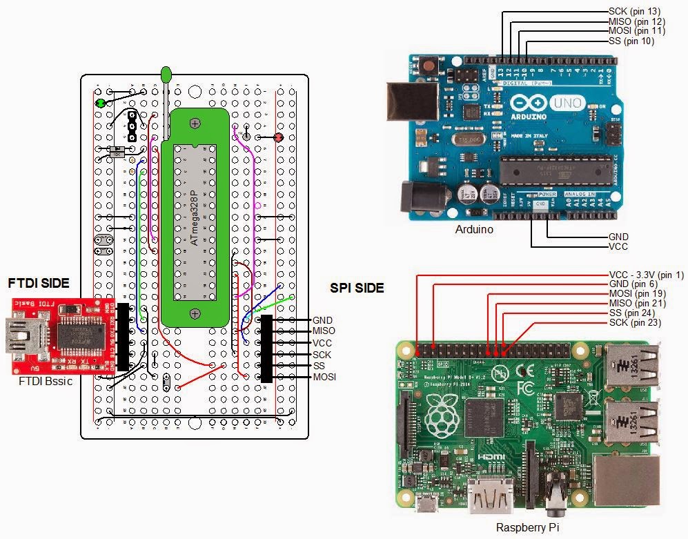
The connector pins labeled SPI are for female - female jumper wires. This interface connects to the Raspberry Pi or to the Arduino Uno. Connections to the Raspberry Pi are to set the fusebits on an ATmega328P, and to load sketches developed on the Gertboard. The connections to the Arduino UNO are only to install a bootloader on an ATmega328P.
Note the interface labeled "FTDI". This interface is used to upload sketches to an ATmega328P (must have the bootloader installed) that I have developed on my Arduino. In addition, it provides access to the Arduino IDE Serial Monitor, allowing us to communicate with a program running on the jig's ATmega328P. FTDI is the name of a chip manufacturer that makes USB to Serial ICs. The FTDI interface on my jig connects to a Sparkfun FTDI Basic breakout board. This small board has a mini USB on one end and a six pin female connector on the other that plugs directly onto my jig.
There is a three pin female connector labeled resonator. Since the Gertboard and the Arduino Uno operate on different frequencies, the connector allows a 12MHz resonator to be connected for the Gertboard sketches and a 16MHz resonator for the Arduino operations.
There are two LEDs on the jig. The green one lights whenever power is applied to the jig. 5V can come from the FTDI board or the Arduino Uno. The Gertboard will supply 3.3V. The red LED is a sanity check and is connected to PB1 of the jig (this corresponds to pin 9 of the Arduino). After loading a bootloader, I can check if I can upload a sketch to a new ATmega528P by running a version of Blink. Anytime I need to check the jig or my connections, I can program that red LED.

Parts List

  • Prototype Breadboard PCB, half size: Adafruit 1609, $4.50
  • ZIP Socket, 28 pin: Sparkfun PRT-09175, $2.95
  • Right Angle Header Strip for FTDI and SPI: Mouser 571-9-103323-0, $2.24 for a strip of 40 pins
  • ATmega328P Microcontroller: Mouser 556-ATmega329K-PU, $3.55
  • Socket strip for Resonators: Digikey 1212-1125-ND, $3.89 for a strip of 64. Perfect socket for resonator pins
  • 16 MHz Resonator: Mouser 520-ZTT1600MX, $0.50
  • 12 MHz Resonator: Mouser 520-ZTT1200MX, $0.50
  • Red LED - clear housing: Digikey C503B-RCN-CW0Z0AA1-ND, $0.15
  • Red Green - clear housing: Digikey C503B-GCS-CY0C0791-ND, $0.24
  • 10μF, 16V Tantalum capacitor: Mouser 581-TAP106K016CRW, $0.53
  • 0.1μF 100V Ceramic capacitor: Mouser 1C20X7R104K100B, $0.18 ea.
  • 1N4148 diode: Mouser 512-1N4148, $0.10
  • 10KΩ Metal Film Resistor: Mouser 71-RN55D-F-10K, $0.10
  • 1KΩ Metal Film Resistor: Mouser 71-RN55D1001F/R, $0.10 ea.
I use LEDs with clear bodies. I anticipate using LEDs in battery powered projects so I want to minimize the current consumed by LEDs. Normally, you calculate the series resistor to deliver about 10ma. of current to drive the LED on. A resistor of about 330Ω is commonly used. The LEDs with the clear housings require much less current so I typically use a 1KΩ series resistor (about 2ma.). Even that can seem too bright, I might try 2KΩ on my next project.

Using the Jig

Diagram used for all situations follows:
Connecting The Programming Jig

Installing a Bootloader

Make connections as in the diagram above from the jig's SPI connector to the Arduino. Make sure there is a 16MHz resonator installed on the jig. Install an ATmega328P on the fixture. By the way, I probably should have mentioned it before, but do NOT use a ATmega328 unless you are capable of adding support for the device in avrdude and the Arduino IDE. The two devices have different signatures so the ATmega328 will not be recognized unless you are capable and willing to make the software changes I mentioned. The two devices are about the same but the "P" version runs at lower power.
Do the following from the Arduino IDE:
  1. Upload the sketch ArduinoISP: Files\Examples\ArduinoISP.
  2. Select the Arduino Uno board (selects the bootloader for the ATmega328P because that is the microprocessor for the Uno): Tools\Board\Arduino Uno.
  3. Select the Arduino as ISP as the programmer: Tools\Programmer\Arduino as ISP.
  4. Install the bootloader: Tools\Burn Bootloader.
That's all there is to it. It takes less than a minute for the process to complete. Once the TX and RX LEDs, on the Arduino, stop blinking, the bootloader is loaded.

Uploading Sketch Via FTDI

Once the boatloader is installed, you can upload a sketch to the jig using the FTDI Basic board. When I plugged my FTDI Basic into my USB port, for the first time, I found that the drivers had already been installed on my Windows 8.1 system. They must have been part of the Arduino IDE installation. If you do not have the drivers, check out Sparkfun's product page for instructions on getting them. The FTDI Basic costs about $15 at Sparkfun.

Raspberry Pi/Gertboard

The Gertboard is a expansion board that connects to the Raspberry Pi's GPIO pins. It has several different circuits useful for interfacing the Raspberry Pi to the outside world. The Gertboard works with all thee versions of the Raspberry Pi (A, B, B+). Here is what the Gertboard offers:
  • ULN2808 containing six open collector outputs, each capable of driving a 500ma. load up to 50V (from a separate power source)
  • MCP4802 dual channel D>A (digital to analog) converter
  • MCP3002 dual channel A>D (analog to digital) converter
  • ROHM BD6222HFP H bridge motor controller (need a separate power source)
  • 12 output buffer circuits
  • 12 input buffer circuits
  • 12 red LEDs
  • 3 momentary switches
  • ATmega328P microcontroller. Running on 3.3V with a 12MHz resonator. All IO pins are available.
The documentation, unbelievably not provided when you purchase the product, is excellent. It can be found here. The manual references C and python programs that can be used to test out each section of the Gertboard. In order to use the ATmega328P, a bit of software must be loaded in the Raspberry Pi. This is also referenced in the manual and is available from Gordon Henderson. Here is a link to his blog. It all just works great. Newark Element14 has the Gertboard for $40. Inexplicably, Sparkfun sells it for $60. On Sparkfun's product page it lists the microcontroller as an ATmega328. It's an ATmega328P.
My jig will look to the Raspberry Pi just like the ARmega328P on the Gertboard. Therefore, if you want to interface an ATmega328P to a Raspberry Pi without using the Gertboard, the same software from Gordon will do the job. Just make the connections as in the diagram above.
Once you upload a sketch, you may need to communicate with the ATmega328P, such as you do with an Arduino. For the Arduino, you use the Serial Monitor function of the Arduyino IDE. You will not be able to do that from the Raspberry Pi, but you can still communicate with the ATmega328P. You connect RX and TX on the FTDI side of the jig to TX and RX, respectively, on the Raspberry Pi. You connect the FTDI TX to pin 10 (RX) of the Pi and FTDI RX to pin 8 (TX) of the Pi. The alternative to the Serial Monitor is to use a terminal program like minicom within a terminal window on the Raspberry Pi. The installation and use of the minicom program is covered in the Gertboard User's Manual.

Going On From Here

Obviously, the jig as it stands, does not have much utility as it only uses one of the many ATmega328P's IO pins. However, the concept can be used to make something more useful. Here is an example of a project in the works:
All of this goes into an enclosure. I will add temperature sensors and a RF transmitter, with antenna. The ATmega328P is mounted in a standard 28 pin socket instead of the Zif socket. A 16MHz crystal provides the clock reference.
Note the FTDI basic board. It's used to communicate with the ATmega328P. This is necessary to tell the LCD what text to display. Once power is applied, the display is blank. I attach the FTDI Basic board, connect it to the PC, via a USB cable, and bring up the Arduino IDE. The sketch is already running on the ATmega328P so I click on the Serial Monitor and am greeted with a request to type a message. Once that is done, the message is displayed in a Time Square Scroll. I can then remove the FTDI Basic board.
Please check out my blog entries of March 7, 2013 to April 18, 2013 for discussions of my LCD projects for the Raspberry Pi. The last two posts, specifically, are about my Times Square Scroll software. I have since converted the software from python to C to run on the Arduino. I'll report on that effort at a later time.

Monday, October 20, 2014

DS18B20 12 Bit Resolution - What does that mean

DS18B20 Resolution

The following is from figure 2 of the Maxim Integrated data sheet: "DS18B20 Programmable Resolution 1-Wire Digital Thermometer"
When the data sheet talks about 12 bit resolution, what do they mean? From the figure above, you can see that two 8 bit bytes are reserved for the temperature measurement. That means there are a total of 16 bits. But, notice there are only 12 unique bits. Bits 11 to 15, of the most significant byte (MS Byte), will always be the same. If one bit is a "1", all 5 bits will be a "1". If one bit is a "0", all 5 bits will be a "0". That is where the 12 comes from: 12 unique bits.
How is that number related to resolution? Of those 12 bits, eight are reserved for the integer part of the number: bit 4 to bit 11. Bit 0, bit 1, bit 2, and bit 3 make up the fractional component. You can choose to have the DS18B20 measure with 9, 10, 11, or 12 bit resolution. If you choose 12 bits, all 12 bits are used in the calculation of temperature. If you choose 11 bits, the least significant bit will always be a 0. If you choose 10 bits, the last two bits will always be zero. If you choose nine bits, the last three bits will always be zero giving you only one fractional bit of resolution.
With nine bits, the least significant bit is bit 3. The value of bit 3 (from the figure above) is 2-1. That is the equivalent to 12 or 0.5. So, nine bits gives you a resolution of 0.5°C.. If you choose 12 bit resolution, the least significant bit has a value of 2-4. That gives you a resolution of 116 or 0.0625. So, 12 bits gives you a resolution of 0.0625°C..
Why would you want to choose anything other than 12 bit resolution? Why not always choose the best? The answer is speed. When asked for a temperature conversion, the DS18B20 takes multiple measurements and averages them before reporting the result. The higher the resolution, the larger the number of measurements go into the average, and the longer time to complete the conversion. The maximum conversion time for 12 bit resolution is eight times the maximum time for nine bit resolution. Here is a chart of resolution in bits, degrees, and maximum conversion time:
Number of Bits Resolution Maximum Conversion Time, ms.
9 0.5000°C 93.75
10 0.2500°C 187.5
11 0.1250°C 375
12 0.0625°C 750

Deriving Temperature From the Register Data - Temperatures below 0°C

The following is Figure 1 from the Maxim data sheet:
I hope it is clear how the decimal value of temperature relates to the binary digital output column when the temperatures are in the positive range. It might not be as clear when the temperatures are negative. Those binary numbers are really signed binary numbers. This means that the most significant bit, bit 11, or in this case, bits 11 through bit 15 (since these five bits are always the same), tell you if the number is positive or negative. If those bits are all "0"'s the number is positive. If those bits are all "1"'s the number is negative. However, that is only half the story. You might think that if +25.0625 is 0000 0001 1001 0001 then -25.0625 could be 1111 1001 1001 0001. But you see from the figure above that is not the case.
As small as the DS18B20 is, it has to have some computing power. Therefore, it shares characteristics with your microprocessor or microcontroller device. These devices all have some electronic circuitry that perform basic functions. One such function is to add binary numbers. Another is to change all the "1"'s to "0"'s and all the "0"'s to "1"'s. That operation is called inverting. A function that is not commonly implemented is circuitry to perform subtraction. That is because it is possible to subtract by using the two circuits I described, adding and inverting.
How would you subtract 13 from 25 without actually performing subtraction. Let's assume we were working with 8 bit signed binary numbers. 25 is 0001 1001. 13 is 0000 1101. Subtracting 13 from 25 is the same as adding -13 to +25. In order to facilitate the subtraction process, devices like the DS18B20 (because they must do some computing) represent negative numbers by what is called the two's complement of the number. The two's complement is formed by using the aforementioned processes, adding and inverting. First we invert then we add 1.
Let's get the two's complement of -13. First, we invert the 0000 1101 to get 1111 0010. Next, we add 1 yielding 1111 0011. When we add that to 0001 1001 (25) we get 1 0000 1100. Since we are using 8 bit signed binary numbers, that lonely "1" on the left gets lost giving us our final result of 0000 1100 which is decimal 12. This is how the DS18B20 represents the binary (and hex) temperatures that are below 0°C: by their two's complement. Let's prove it. If +25.0625 is 0000 0001 1001 0001. What is -25,0625 in two's complement? Let's invert 0000 0001 1001 0001 to 1111 1110 0110 1110 and add 1. This gives us 1111 1110 0110 1111, which is what is shown in the figure above.
If you want more information on two's complement, including some theory, I recommend this site.

Calculating Temperature From DS18B20 Register Values

When you get the results from the DS18B20, two bytes from the scratchpad, how do you convert them to temperature? Without getting theoretical, this is what I do:
  1. Multiply the value of the most significant byte (scratchpad byte 1) of the temperature data by 256.
  2. Add to the result of step 1, the the value of the least significant byte (scratchpad byte 0).
  3. Check to see if the temperature is negative by testing if the result from step 2 is over 127. If so the temperature is negative.
  4. If the temperature is negative, subtract the result of step 2 from 65536.
  5. Divide by 16

Sunday, July 13, 2014

Cyclic Redundancy Check (CRC) of DS18B20 Serial Data

This is a continuation of my last three blog posts.
Maxim has application note 27, "Understanding and Using Cyclic Redundancy Checks with Maxim 1-Wire and iButton Products", that I will refer to here. You can see this here.
If you transmit data from one place to another you want to know that the data arrived unchanged. The cyclic redundancy check is the best way to tell you if the transmission was successful.
We transmit serial data from two sources within the DS18B20: from its Read Only Memory which has the ROM code stored, and from the scratchpad memory. Basically, while transferring data to us, the user, the DS18B20 looks at the data it is sending, one bit at a time, and makes a calculation. The result of that calculation is an additional byte that is tacked on to the data stream. The value of this byte depends solely on the bits that have preceded it in the transmission. This additional byte is the CRC byte. The ROM code is actually 7 bytes long but the CRC byte makes it 8 bytes long. The scratchpad data is 8 bytes long and its CRS makes it 9 bytes long.
My code calculates the CRC as each bit of each byte is received. One of the nice things about CRC, and, this should be kept in mind, is if the transmission was successfully received, my calculation of the CRC will be 0. It's very easy to check for 0 in code. Any result besides 0 means the transmission failed.
How do you calculate CRC? It's hard to put that into words. The mechanism for calculating CRC is generally expressed as an electronic circuit. You can actually build this circuit and calculate the CRC, or you can emulate this circuit in software. I have done the latter in my One_wire_DS18B20 library file. I was surprised how few lines of code it took to write the CRC function. More on this later.

Getting Into Electronic Hardware

Here we go diving into interesting waters. But, I don't know how to otherwise discuss how this all works. So here we go. Maxim gives a representation of the electronic circuit in it's figure 2 of the application note. Here it is:
I have my own version of that figure that shows more detail, especially what is in those boxes called stages:
There are two different kinds of parts here, the boxes are called flip-flops (No connection to the ones you wear to the beach). Let's look at a flip-flop a little more closely:
Why the funny name, flip-flop? The name describes the functionality, perfectly. The output from the part can be made to flip from one state to another. That is, from a high voltage to a low voltage; or, stated another way, from a logic HIGH state to a logic LOW state; or, stated yet another way, from a "1" to a "0". Of course going back in the other direction is just as easy. Flip-flops make up a large part of the circuitry in your computer microprocessor. There are thousands of them. The simplest can be constructed with just two transistors. The flip-flip we are showing here is a bit more complex and is called a D flip-flop. Below the flip-flop, is a timing diagram that plots voltage (vertical) against time (horizontal). When the voltage is at it's high state we call this a logic "1". When the voltage is near 0 volts, we call this a "0". (That is arbitrary, we could call a high voltage a "0" and a low voltage a "1").
We see three signals, or waveforms: "Data", "Clock", and "Output" (we are going to ignore reset). "Data" is the information that is being transmitted serially, one bit at a time. "Clock" is another signal, and when it makes a transition from a "0" to a "1", the logic level the device sees on its "D" pin, will appear at its "Q" pin. We show that the data on the "D" pin is "latched" on the rising edge of "Clock" by those upward arrows on the "Clock" waveform. The first time we see "Clock" going from a low to a high, the "Data" happens to be high (or a "1"). After a really short delay, that "1" appears at the output of the flip-flop. That little delay is important. It is not obvious why here, but will be when we consider more than one flip-flop. If you look at each rising transition you will see the output will mirror what is at the "D" pin. So far, not so interesting. But. wait, let's connect a second flip-flop to the first one.
We connect a second D flip-flop so that its "D" ("D" for data, by the way) pin connects to "Q" of the first one. "Clock" connects to both flip-flops. Now we can see why that little delay is important. When we look at the second time the "Clock" goes from low to high, we see that the "D" pin of the first flip-flop is low, so the output of the first flip-flop wants to go low to follow the input. However, there is a slight delay so it stays high for a little while longer. If that delay was not there, the output of the first flip-flop would be changing at the exact time that "Clock" is latching the data at the input of the second flip-flop. What would the output of the second flip-flop be? A "1" or a "0"? Who knows! That little set-up delay assures that the input of the second flip-flop is a "1" long enough so the "Clock" latches a "1" at the output of the second flip-flop.
Is this circuit any more useful than the first? The usefulness of the circuit will be evident if we add more flip-flops. Let's have a total of 8:
Remember, "Data" is the information coming into the circuit one bit at a time. "Clock" captures that information in the first flit-flop. As new bits arrive, they cascade to the other flip-flops from left to right. Each rising edge of "Clock" shifts the information on "Data" from flip-flop to flip-flop. Thus, this circuit is called a shift register. The flip-flop outputs are labeled "Q7" - "Q0".
The circuit is also called a serial to parallel converter. After shifting in the serial data enough times to get the first bit cascaded down to the last flip-flop, the original eight bit data word is available on "Q7" - "Q0" in parallel format. We could connect "Q7" - "Q0" to other circuitry if we wished.
Why the grayed out areas? We don't have enough information to know if the logic levels in these areas are a "1" or a "0".
My project emulates the shift register in software. Every time we ask for data from the DS18B20, we call on a couple of functions in my 1_Wire library. We emulate "clock" with a "for" loop to shift in each bit of each byte. The "Q7" - "Q0" outputs are represented by an eight bit variable. We call that loop enough times to capture each byte in the message from the DS18B20.
As we shift in each bit, we do a calculation to determine the CRC value. We continue that calculation until the last bit of the last byte of the message has been shifted in from the DS18B20. For example, if we were capturing ROM code, we would capture eight bytes. The last byte of the ROM code is the CRC value (calculated by Maxim). After shifting in all 64 bits, the result of our calculation should be "00000000" (Recall my forth paragraph above).

Enough Background - Getting To The Cyclic Redundancy Check

Let's repeat that figure at the top of this post:
Notice that this is similar to the shift register above. We have added three parts called exclusive OR gates. They each have two inputs on the left and one output on the right. The exclusive OR is one of a series of logic circuits. Some of the others are inverters (also called NOT gates), AND gates, and OR gates. These devices look at the logic levels at their inputs ("1" or "0") and decide what the logic level of their output will be. The output of the inverter is opposite of the input. The output of the AND gate is "0" unless all the inputs are "1". The output of the OR gate is a "1" if any of it's inputs are "1". The output of the exclusive OR gate will be "0" if the logic level of the inputs are the same (both "0" or both "1"). If the inputs are different ("0", "1" or "1", "0") the output will be a "1".
That CRC circuit seems to be a bastardized version of the shift register. The output from the last stage is fed back into the circuit. This circuit is specific to the way Maxim handles the CRC for devices that transfer data in eight bit bytes. They have a different circuit for devices that transfer 16 bit bytes. That circuit has 16 "stages"
The type of CRC circuit is also know by its polynomial, a mathematical expression representing the number of stages, and where, and, how many exclusive ORs are in the circuit. The polynomial for our circuit is shown on the figure above from Maxim's application. It is X8 + X5 + X4 + 1. This means we take the output of the forth, fifth, and eighth stage as inputs to our exclusive OR gates. There are other schemes with different number of exclusive OR gates that feedback to different stages. These have different polynomials.
The mathematics of the cycle redundancy check is quite involved and I won't begin to discuss it here. There is plenty of in-depth information on the web. Let's move on to the final discussion of implementing the CRC in software.

Calculating the CRC in Software and in Our Equivalent Circuit

The following code is taken from my calculateCRC_byte function found in my One-Wire_DS18B20 library.
The Equivalent CRC Circuit diagram contains the value of the CRC in the eight bits of "Q7" - "Q0". Note, however, the sketch variable "CRC" is an int, not a byte, making it 16 bits long. The reason "CRC" is 16 bits long is due to lines 11 and 14 of the sketch. On those lines, "CRC" is operated upon by a value that is nine bits long. Hence, "CRC" must be longer than 8 bits. When we reach the bottom of the function, the top eight bits of "CRC" will always be "00000000". The lower eight bits will be equivalent to "Q7" - "Q0" in the circuit. The top eight bits will also be "00000000" when we arrive at the "IF" statement in line 10.
The sketch has two loops, an outer loop for the number of bytes we send to the function, and an inner loop that runs eight times, once for each bit of the incoming byte, "inByte[i]".

Lines 9 Through 15 of the Code

Comparing the equivalent circuit to the sketch, the "IF" statement in line 10 implements, exactly, the exclusive OR gate on the left of the equivalent circuit. Let's look at that statement closely:
"if ((CRC % 2) ^ (inByte[i] % 2)){"
The "%" operator is called a modulo. The result of the modulo operation is the remainder after dividing whatever is to the left of the operator by whatever is to the right of the operator. In this case, we divide the current value of the variable "CRC" by 2. If the value of the variable "CRC" is even, the modulo will be "0". If odd, the module will be "1". Whether or not "CRC" is even or odd depends solely upon the value of its least significant bit (last bit on the right). Therefore, the value of "CRC % 2" is the value of the least significant bit of "CRC".
The CRC Equivalent Circuit holds the value of the CRC on its outputs "Q7" - "Q0". Applying the same argument as in the last paragraph, "CRC % 2" is the value of "Q0", the least significant bit of the CRC stored in the flip-flops.
Using what we learned above, "inByte[i] % 2", will give us the value of the least significant bit of the data byte, "inByte[i]". This is exactly the same as the current value of "Data" in the CRC Equivalent Circuit.
The symbol "^", in the "IF" statement, sitting between the two modulo expressions, is the bitwise exclusive OR operator. Because, "Q0" and "Data" connect to the exclusive OR at the left of the equivalent circuit, the entire "IF" statement is equivalent to that same exclusive OR gate. The result of the "IF" statement is precisely the same as the output of the left-hand exclusive OR gate. From our discussion of how the exclusive OR works, if the value of the least significant bit of the variable "CRC" and the value of the least significant bit of the array "inByte[i]" are the same (both "0" or both "1"), the result of the "IF" statement will be "0", otherwise (one is a "0" and the other a "1") the result will be a "1". In the same manner, if the value of "Q0" and the value of "Data" are the same, the output of the exclusive OR gate in the equivalent circuit will be "0". If different, the value will be "1". This output is the input to the first flip-flop at the left of the circuit, and one of the inputs of the other two exclusive OR gates in the equivalent circuit.
We described of the exclusive OR gate as being a "0" if its inputs were the same and a "1" if they were different. We used that description to evaluate the "IF" statement and the output of the exclusive OR at the left of the equivalent circuit. There is another useful way to look at an exclusive OR gate, and we will use that way in the following discussion. We can look at one input of an exclusive OR as a control input that controls the relationship between the second input and the output of the gate. If this control input is a "0", the output of the exclusive OR will follow the other input. If the control is a "1", the output will be opposite of the input (A "0" becomes a "1" and a "1" becomes a "0").
The result of the "IF" statement controls which of the two operations we apply to the value of "CRC" (either line 11 or line 14). We either exclusive OR "CRC" with "100011000" or "000000000". In our new way to look at the exclusive OR gate, those two series of nine bits are the control inputs to nine exclusive OR gates. They control what happens to value of the variable "CRC" at that point in the sketch. We can call them a control word.
Let's operate on a sample byte to see what those control bits do:
011010101 Sample 011010101
000000000 Control Word 100011000
011010101 Result 111001101
Note that when the control word is "000000000", there is no change to the sample, the result is the same as the sample.
I said the nine bit control word was like having nine exclusive ORs. But, six of those bits are always "0", both in line 11 and line 14. Consequently, we can replace those six exclusive ORs with direct connections, meaning there are only three exclusive ORs. This happens to be the same number of exclusive OR gates in our equivalent circuit. In fact, they are in the same relative positions. The most significant bit of our control word corresponds to the left-hand exclusive OR gate. The two bits of the control word that can change, are in exactly the same place as the other two exclusive OR gates in the circuit.
The purpose of the exclusive ORs are to modify the value of CRC existing at "Q7" - "Q0", or the value of the variable "CRC", before there is further processing. If the control word is "000000000", there will be no change in the value of "CRC". Since, the effect of exclusive ORing "CRC" with "000000000" is no effect at all, lines 13 - 15 of the sketch are superfluous. They do not appear in my actual code. I only added them here because it made explanations easier.
Let's look at the output of our exclusive ORs, be they in the sketch or the equivalent circuit. Exclusive ORing with "000000000" was the result of the output of the "IF" statement being "0". Let's see what happens to the equivalent circuit when the output of the left-hand exclusive OR is "0". First, the input to the left-hand flip-flop will be "0". The output of the left-hand exclusive OR also connects to an input of the other two exclusive ORs. Let's consider the output of the left-hand exclusive OR to be the control input to the other two flip-flops. If this control input is "0", the output of the two flip-flops ("Q4" and "Q3") will be the same as their other inputs, meaning there will be no change to the CRC.
When the output of the "IF" statement is "1" we will modify the value of the variable "CRC" with "100011000". At the equivalent circuit, the output of the left-hand exclusive OR will be a "1". The effect will be that the input of the left-hand flip-flop will be "1" and the control input to the other two exclusive ORs will be a "1". This will cause the "X4" to be of the opposite logic level of "Q4" and "X3" to be of the opposite logic level of "Q3". In other words, we have flipped those two bits.

Lines 16 and 17 of the Code

"Whew", we now have the variable "CRC", and the inputs of those flip-flops, set up for the next operation.
In the equivalent circuit, the signal labeled "Clock", which has been at "0" will briefly go to a "1" and back to "0". As in our discussion of the shift register, the logic level at the inputs of those flip-flops will now appear at the outputs of the flip-flops. This has the effect of shifting the current value of CRC down one position. Sometime after that, the value of "Data" will have the next bit of the serial data coming into the circuit.
Our sketch has an exact equivalent to the "clock" signal. That equivalent is line 16: "CRC >>= 1;". This operation will take the value of "CRC" and shift all 16 bits down one bit position to the right. A "0" will be shifted into the most significant bit of "CRC".
The next line, line 17, shifts the eight bits of "inByte[i]"down one bit to the right. A "0" will be shifted into the most significant bit. The operations of lines 16 and 17, are directly comparable to applying the clock to the flip-flops, and introducing the next data bit, in the equivalent circuit.

An Example

Let's take an example of two bytes and walk them through the sketch. Let's assume the two bytes are "10110100" and "01010011". If I run "10110100" through the sketch, by itself, the resulting CRC will be "0000000001010011". If we ignore the top 8 bits, the CRC is the same as the second byte we will pass to the sketch. Since the second byte is the same as the CRC of the first byte, the final CRC should be "0000000000000000", after processing both bytes.
First Byte 1:
i j inByte[i] CRC CRC Before Right Shift
0 0 10110100 0000000000000000 0000000000000000
0 1 01011010 0000000000000000 0000000000000000
0 2 00101101 0000000000000000 0000000100011000
0 3 00010110 0000000010001100 0000000010001100
0 4 00001011 0000000001000110 0000000101011110
0 5 00000101 0000000010101111 0000000010101111
0 6 00000010 0000000001010111 0000000101001111
0 7 00000001 0000000010100111 0000000010100111
0 7 00000000 0000000001010011 <-After the Final Shift
Now Byte 2:
i j inByte[i] CRC CRC Before Right Shift
1 0 01010011 0000000001010011 0000000001010011
1 1 00101001 0000000000101001 0000000000101001
1 2 00010100 0000000000010100 0000000000010100
1 3 00001010 0000000000001010 0000000000001010
1 4 00000101 0000000000000101 0000000000000101
1 5 00000010 0000000000000010 0000000000000010
1 6 00000001 0000000000000001 0000000000000001
1 7 00000000 0000000000000000 0000000000000000
1 7 00000000 0000000000000000 <-After the Final Shift
The DS18B20 transmits data least significant bit first. If you had an application that transmits most bit significant first you would have to modify the "IF" statement. Assuming the data coming in is 8 bits in length, you could replace "inByte[i] % 2", with "inByte[i] > 127". Also, "inByte[i] >>= 1" would be replaced with "inByte[i] <<= 1". If the CRC is calculated using a different polynomial, you would have to modify line 11 accordingly.
Feel free to download and experiment with this sketch. You can enter as many bytes as you wish. Just add some print statements and setup() and loop() to feed the function.

Monday, July 7, 2014

DS18B20 Connected Using Parasitic Power

This is a continuation of my last two blog posts.

Parasitic Power and 1-Wire Devices

The 1-Wire devices have three pins, one for power, one for ground, and one for data. However, it is possible to connect the device without connecting to a source of power. In that case, both the ground and power pins are connected to ground. That simplifies cabling as it is only necessary to run two wires instead of three. A device connected in this matter is said to be connected using parasitic power. The device gets its power, parasitically, from the data line. And, the data line is powered through a 4.7K pull-up resistor to the power source (5V for the Arduino). That relatively high value of resistance still allows the Arduino or a DS18B20 to pull the data line to a low logic state (near ground). That arrangement is sufficient to power the device for all operations except when the device is undergoing temperature conversion and when writing from the scratchpad to the device's EEPROM (not the ATmega EEPROM). For those operations, the device may draw as much as 1.5mA. That's not a lot of current, but still more than can be supplied through that pull-up resistor. For those two operations, we connect the data line, directly, to the power source. Of course, once we do that, we can't have any other operation going on that requires a transfer of data in either direction (can't pull the data line low).

Parasitic Power Control Circuit

Obviously, we need a switch to control when we connect the data line to the power source. The switch I devised can be seen in the figure below:
My switch is the 2N5087 PNP transistor. Why that transistor? I just happened to have a couple. The transistor can supply about 100ma., so more than 67 parasitically connected devices could sit on the bus. Sparfun has a 2N3906 which should work just as well. Actually, this one will sink 200ma. If you are interested, Sparkfun has a tutorial about how transistors operate. Look here.
Once a low voltage (near 0) is applied through the 1K resistor to the base of the transistor, the transistor "turns on" making a near short circuit between the collector (connected to the power source) and the emitter (connected to the the data line). I use an Arduino pin to control the transistor (PB1 in my case). When I want the switch to be off, I program PB1 to be an input. As an input, the Arduino can not supply any current to the transistor's base-emitter junction so the transistor can not turn on. When I want the switch on, I program the logic level at PB1 to be LOW and program the pin to be an output.

Detecting Devices Connected Using Parasitic Power

It is not necessary to keep track of the devices that are connected using parasitic power. You can use the library function command read_power_supply(). Like all function commands it must be preceded by initialization(), and either match_rom() or skip_rom(). Function match_rom() will address only one device - the one with the ROM code you pass to it. If that device is connected with parasitic power it will pull the data line low. If skip_rom() is employed, ANY device connected with parasitic power will pull the data line low.

Programming Consequences of Devices Connected Using Parasitic Power

In my library function Convert_t(), if a device is not connected using parasitic power, I let the device inform my code when the convert operation is complete. The device will pull the data line to a logic LOW while the conversion is taking place. My library function reads the data line every millisecond. When a logic HIGH is read my code can move on and do its next operation. According to the data sheet, the resolution at 12 bits should take no more than 750ms. I found that the conversion is done in about 550ms. at 12 bit resolution.
If using parasitic power, the device can not pull the data line low because of the hard pull-up. The only option is to pass the resolution to the convert_t() function and use a delay() statement to give the device enough time to make the conversion. To be sure enough time is given, I use the specification in the data sheet.
You can look at my Read_Temperature.ino sketch to see more of my implementation of parasitic power. It is one of my files on GitHub, but you can see it here.

Saturday, July 5, 2014

My 1-Wire Arduino Library for DS18B20 Temperature Sensor

This is a continuation of my last blog post.

The Include File For the 1-Wire DS18B20 Library

This 1-wire library will work equally well with an Arduino and a Gertboard.
At the top of the file are #define statements to account for your hardware set-up. Unless you use the same hardware choices I made, you make the appropriate changes to the file and save the file.
The first #define is for CLOCK_FACTOR. I reported in an earlier post that the delayMicroseconds(), Arduino IDE, function is not accurate when using the Gertboard. I tested this thoroughly, at different values, using an oscilloscope. My results show that you must divide the desired delay by 0.67 to get an accurate delay. Consequently, if you use the Gertboard, make the clock_factor 0.67. Select 1.0 for the Arduino. The difference is caused by the 12MHz clock frequency of the Gertboard compared to 16MHz of the Arduino. The delay() function requires no correction.
The rest of the #defines relate to the selection of the two Arduino data pins you select. One pin is the data pin for the 1-wire bus, and the other is the pin that controls the transistor for parasitic power. I will have a post devoted to the parasitic power transistor circuit. Hopefully, my comments, in the file, are enough to guide you through the selections.
If you use the Gertboard you can take the pin names as they appear by the J28 connector (PB1 for example). These are the same designations as used in the ATmega's data sheet, and, more importantly, the same designation as used in the avr/io.h include file. If you use the Arduino, where pin numbers are 0 to 13, you will need to convert them to the ATmega numbers.
Arduino ATmega Arduino Atmega Arduino Atmega
0 PD0 5 PD5 10 PB2
1 PD1 6 PD6 11 PB3
2 PD2 7 PD7 12 PB4
3 PD3 8 PB0 13 PB5
4 PD4 9 PB1
The rest of the file declares the functions in the library source file. These are the public functions, those that can be called from a sketch, and the private functions, those that are not available from sketches.

The Soruce File For the 1-Wire DS18B20 Library

Most of the functions are short. Their comments are longer than the code. You will have to be familiar with ATmega register programming and bit manipulation. I have tutorial on useing direct register programming here.
In the next several posts, I'll go into some detail on the search_device() and calculateCRC_byte() functions. But, first, I need to address parasitic power and what to do about it. That's next.

Sunday, June 15, 2014

DS18B20 Temperature Project For Gertboard/Arduino

Some time ago I became rather fascinated with the Maxim/Dallas DS18B20 temperature sensor. I bought a couple and connected them to my Pi. This blog has tracked my progress with the little device, starting with the four posts of June of 2013:
Then, the October, 2013 post: Finally, the November, 2013 addition:
That project became very useful and I learned a lot. However, I had a couple of issues. I did not think it was suitable to tie up a general purpose microprocessor (the Pi) with a connection to a couple of sensors. I was disappointed that the driver did not support all functionality of the device like choice of resolution. There also seemed to be a stability issue. About half of the measurements resulted in a CRC failure requiring measurement repetition.
I thought the sensors should really connect to a microcontroller like the ATmega328P. Once programmed, the microcontroller could be lifted off the programmer and placed in its own circuit board in an enclosure. I did this for my camera remote control project back in January of this year.
Thus was born my concept for a very involved project. Here are the design parameters I set for myself:
  1. Connect multiple sensors to an ATmega328P microcontroller.
  2. Design for a hypothetical industrial application where many DS18B20 temperature sensors may be employed.
  3. Store the 8 bit ROM code and a 12 character (max) description for up to 50 devices.
  4. Use the ATmega's 1 kbyte of EEPROM to store the ROM codes and descriptions.
  5. Use the Arduino IDE to develop the code.
  6. The "programmer" will be the Gertboard connected to the Raspberry Pi.
  7. Write my own 1-Wire interface library incorporating all of the DS18B20's functions found in its data sheet.
  8. Remove the ATmega microcontroller from the programmer and install it on a circuit board within an enclosure.
  9. Connect a 16 character by 2 line LCD display to the microcontroller to display temperature and device number.
  10. Connect several switches to the microcontroller for simple menu control.
  11. The microcontroller and the Pi to communicate wirelessly.
  12. The Pi will serve as a "front end", with a menu driven choice of operations to be carried out by the microcontroller.
  13. Temperature measurements returned by the microcontroller to be graphed by the Pi using RRDtool.
I've been working on items 1 - 7.
If you are interested in this project it is important to be familiar with the DS18B20 device and the 1-Wire interface. Maxim has an excellent data sheet describing the functionality, programming commands, and timing requirements. It can be found here.
I wrote my own 1-Wire library for Arduino/Gertboard. You may ask why since the Arduino IDE comes with a 1-Wire library already included. I simply wanted the challenge of doing it. I also wanted to present the library to others with code and comments that anyone can understand. However, if you use the Arduino built-in functions like pinMode(), digitalWrite(), and digitalRead() to control your microcontroller I should tell you that I do not! I use ATmega direct register programming. I have tutorial at this blog entry that explains the difference and how to use direct register programming.
My 1-Wire library only covers the DS18B20 temperature device. If it covered all of the Maxim devices, I would have to purchase one of each and test that it works with my library. I'm not going to do that - I'm only interested in the temperature sensors. There are a couple of other temperatures sensors and they probably will work with my library. Actually, there does not seem, to me, to be a reason to use any of the other Maxim temperature sensors. I could not see any advantage to them. At present, my library is not quite complete. Here is the status of the functions I have completed. The names are taken from the command names in the data-sheet:
  • Initialization - Done
  • Search Rom - Done
  • Read Rom - Done
  • Match Rom - Done
  • Skip Rom - Done
  • Alarm Search - Done (updated July 3)
  • Convert T - Done (updated June 18)
  • Write Scratchpad - Done
  • Read Scratchpad - Done
  • Copy Scratchpad - - Done (updated June 22)
  • Recall E2 - - Done but not tested (updated June 22)
  • Read Power Supply - - Done (updated June 22)>
  • Compute CRC (this function is not listed as a separate command in the data sheet) - Done
I have not incorporated parasitic power. This really only effects Convert T at this time. I will get to that after I sort through my supply of old parts and find a suitable transistor to pull up the bus connection to Vcc. When that occurs, I will augment Convert T to handle parasitic power. I plan to complete the four functions I have not started. I have incorporated parasitic power into the project as of June 18.

A disappointment with the Gertboard and the ATmega EEPROM

I simply could not store data in the ATmega's EEPROM when the ATmega is installed on the Gertboard. After writing to an EEPROM address, a read of that address always resulted in reading 11111111 - which is the cleared state. I spent about a week trying various programs. Nothing worked.
I explained my problem on the Classic Gertboard section of the Raspberry Pi forum. A very knowledgeable fellow from the Netherlands really tried his best to help me out. We had quite a few conversations on the forum. Gert van Loo, the developer of the Gertboard chimed in a couple of times. I really thank them for their help. Ultimately, nothing worked for me. I think the one person who could have solved the problem, Gordon Henderson of Gordon Projects, did nor respond to my email. Gordon developed the means to use the Arduino IDE with the Gertboard.
I really wanted this EEPROM access to work so I purchased an Arduino Uno, mainly just to see if my code would work at all. I connected the Arduino to the Pi and used the same Arduino IDE as I used with the Gertboard and it all just worked. My guess as to why it does not work with the Gertboard is the difference in how a sketch is uploaded to the ATmega chip. With the Arduino, one selects "Upload", but with the Gertboard, "Upload Using Programmer" is used. I have a feeling that the latter clears the EEPROM (writes all 1's to all bytes) before uploading. Now, one of my design parameters has changed. The project is off the Gertboard and onto the Arduino. Furthermore, my Arduino is now disconnected from the Pi and connected to my Windows PC. I take advantage of the much faster environment, ease of printing, and easier access to my githup repository allowed by the PC.
As of this time, I have the library mostly written, as I discuss above. I wrote several Arduino sketches to check out the library and make the sensors useful. Now, everything runs on the Arduino - the Raspberry Pi is not involved. I have not added the lcd device - that will be next.

Github Repository - Library and Sketch Files

I spent about a day learning about github and created a repository for this project. The repository can be found here.
The repository includes three libraries:
  1. EEPROM_Functions library - functions used to read from and write to the ATmega EEPROM.
  2. InputFromTerminal library - to input floating point or integer numbers from the serial monitor.
  3. One_wire_DS18B20 library - all the ROM Commands and DS18B20 Functions as called out in the DS18B20 data sheet.
In the repository, the directory "DS18B20_Temperatur_Sensor" contains the sketches to read temperature, scan for new devices, and manage the devices in EEPROM, etc. They include the following individual sketches:
  • "Read_Temperature" - Asks user what devices to run, number of measurements, and time between measurements. Function determines if devices are connected using parasitic power. Measurements are made accordingly. User has the option to print out the temperature limits as well as the resolution along with the temperature. Once the run is made, displays the average of all measurements for each device. If there were any CRC errors or initialization errors, the number of these are reported. If a device is connected using parasitic power, when the device is undergoing the convert temperature process, a transistor pulls the 1-wire data line up to Vcc. The time for this "hard pullup: is dictated by the data sheet for the resolution programmed into the device's scratchpad. For devices not connected by parasitic power, when undergoing temperature conversion, the device, itself, informs the bus when the conversion is done.
  • "Scan_for_Alarms" - Scans the 1-wire bus to see if any device's temperature is out of limits. If so, displays that information to the user. This function must determine if the device is connected using parasitic power.
  • "Find_New_Device" - Scans the 1-wire bus to see if any device has been added. If so, asks user for a description which is stored in ATmega EEPROM along with the ROM code. Asks user to input upper and lower temperature limits and resolution. These are stored within the device's scratchpad and the device's EEPROM
  • Devices_On_The_Bus - Uses library search_rom() to report to the user all devices it finds on the 1-Wire bus along with their ROM codes. It also reports the result of the CRC of the ROM codes.
  • "Devices_in_EEPROM" - Displays all devices in the EEPROM along with their descriptions.
  • "Edit_Stored_Information" - Reports to user the ROM code, description, upper and lower temperature limits and resolution for each device on the 1-wire bus. Asks user which device to change and what to change. Changes are made accordingly, and stored.
  • "Remove_Device_From_EEPROM" - Allows user to remove ROM code and description for any device from the ATmega EEPROM. This does not remove information from the device's scratchpad or the device's EEPROM.
I had hoped to combine all of the above sketches into one sketch with a menu that allowed the user to select the functionality that each individual sketch provided. I actually created that sketch but when compiled, I found I exceeded the memory space allowed for variables. I exceeded the memory space due to the large amount of text associated with print statements. I felt these print statements are more important than a menu driven capability so I abandoned that approach. It is necessary to bring up, compile, and run each sketch individually.
Also, at the top level of the repository there is the directory "EEPROM Sketches". Under here you will find several sketches used to manipulate data in the ATmega EEPROM. These sketches were used to assist with other code development and troubleshooting.

Couple of Final Comments

As I said, previously, it was very common to have CRC errors when controlling these sensors from the Raspberry Pi. After making many thousands of measurements, with the Arduino controlling the sensors, I have received no initialization or CRC failures.
Just to reiterate, everything is written for the Arduino IDE. They are in the repository in such a manner that they can be downloaded directly. The libraries will have to be placed into your Arduino\libraries directory for them to be recognized.
My next blog entries will delve into details of some of my code.

Tuesday, May 13, 2014

Arduino Libraries - DON'T DO THAT!

Don't do what? Well, lets lead up to the answer to that question.
I wrote a fairly long library .cpp file (and, of course its .h file). It worked just fine in my sketch. But, I decided to make some changes. Not wanting to lose what I had (I knew it worked) I made copies of both the .h and .cpp files, appending "save" to the file name for each of the two files. I had four files: something.h, something_save.h, something.cpp, and something_save.cpp. All four files were under home/pi/sketchbook/libraries. I wanted to minimize the changes to my sketch (.ino file). Therefor, I did not want to change any of the function names in the library files. I made my changes, and compiled the sketch. The result: I received a list of compiler errors that went on and on and on.
To illustrate what happened, I repeated the sequence of events with a really small, and trivial example:
The only differences I made were to append a "+ 1" to "c = a + b" in the original .cpp file, just to make something different, and to append "_save" and "_SAVE" to the top lines of the bottom two files. I compiled the sketch and you can see what occured:
That's a lot of error messages for a tiny example sketch. I know it's a little hard to read the error messages because of the red text. Here is what it says:
Mylibraries/ridicules.cpp.o: In function RIDICULES::addNumbers(int, int)':
/home/pi/sketchbook/libraries/Mylibraries/ridicules.cpp:8 multiple definition of RIDICULES::RIDICULES()'
Mylibraries/ridicules_.cpp.o:/home/pi/sketchbook/libraries/Mylibraries/ridicules_save.cpp:8> first defined here
Those three messages are repeated three times. Please note I created a directory under home/pi/sketchbook/libraries called "Mylibraries". I stick my libraries there to separate them from the ones that came pre-installed with the IDE.
Note what I have colored red. This is reference to my ridicules_save.cpp file. My sketch does not reference "ridicules_save". Why is "ridicules_save" part of the build? To start to understand things, I did a search for the object files (".o") referenced in the compiler errors. I knew they were not in the Mylibraries directory. Here is what I found:
Note that all of these object files were created at the same time. They are all created every time you compile.
The IDE generates an object file (with an .o extension) of every .cpp file it finds in Mylibraries. It also makes an object file of .cpp files not in the sketch/libraries path. These ".o" files are needed to support Arduino functionality. There are other .cpp files in the sketch/libraries path that are skipped. This includes, for example, OneWire.cpp. Perhaps these are not included because I have never compiled a sketch using them.
I would have thought the IDE would only make an object file of the .cpp files you call for in your sketch and not all the others in your directory. But it does, so now that we know we can answer that question at the top:
Don't have more than one .cpp file with functions that have the same name in the libraries directory. If you need to keep copies of older versions of library files stick them in a directory outside of /home/pi/sketchbook/libraries.
By the way, you can have two files with addNumber() functions, just not two RIDICULES::addNumbers functions. Make one VERY_RIDICULES::addNumbers and you will be OK.

Tuesday, March 18, 2014

Writing An Arduino Library

My last post included a script for controlling the angle of rotation of a small dc servo. That script expects the user to input a floating point number from the terminal. I wanted that script to concentrate on the servo code, so to avoid encumbering the script with the process of handling the user's input, I put the input handling code into a library. Never having created a library, I wanted to learn how that is done. I read several tutorials but they all seemed rather simplistic. One of my concerns was how to pass values between the code that uses the library and the library functions themselves. I started with simple functions and built on those until I arrived at the function I needed for the servo
When you use the Arduino "Serial.read()" function to read from your terminal, you get only one character from each call. If you need more than one character, you need successive reads and a way to put those characters together into something meaningful. You also need to know when the last character was entered and some way to deal with characters entered in error. My servo script wants the user to input positive or negative floating point numbers of indeterminate length.
Note added June 22, 2014 concerning the last paragraph. If you use an Arduino instead of the Gertboard, you can use the serial monitor provided by the Arduino IDE. This serial monitor works quite differently. Rather than only returning one character for each call, it buffers your key presses and returns all of the characters when you hit "enter". In switching my next project from the Gertboard to the Arduino I had to modify the library created below to accommodate this change. See my post of June 15, 2014.

Final Script

Figure 1 below is my final script to control the servo. This is the same as in my previous post. The leading comments in that script were all about making the servo work so I removed them here. This script uses the library I wrote. You cannot see any of the details associated with inputting the floating point number. Only two lines, 2, 4, and 26 deal with the library:
FIGURE 1: Final Script - Without Leading Comments

Getting Started Making A Library

First, you develop the code, as usual, in a script using the Arduino IDE. Identify the parts of the code that will eventually be part of your library: functions, commands, and variables. Make sure there is test code that thoroughly tests the soon-to-be library. Compile and upload this script to make certain it will run properly. Try to break the code by changing conditions.
My test code is the code to control the servo. Figure 2 is my script. I call it my all inclusive script because it contains everything, in one script: the code to input numbers and code to control the servo:
Figure 2: Original All Inclusive Script - No Leading Comments
Most of the code (lines 3 to 68) deals with inputting the floating point number and just a few lines with the servo control.
The code to handle inputting the number accepts any digit, accepts a minus sign only if it is the first character, accepts one, and only one, decimal point, and accepts the backspace key to make a correction. All other characters are ignored. The function returns the floating point number to the calling code. This is not a perfect solution. I don't have a way to correct individual characters. When the backspace key is pressed, a space prints on the terminal after the last character, and the entire number must be entered from scratch.
I think it is pretty clear how the code works so I won't dwell on the details. We have two functions "termNumb()" and "clearVars()", and several variables. "clearVars()" is only called from "termNumb(). "termNumb()" is called from the program in line 91. The variables (lines 3 - 5), one int, three floats, and three boolean are needed by both functions so are global.

Now We Give The Code Some Class

Now that the code is working and tested as thoroughly as possible, it is time to define a class. We will tie those soon-to-be library functions to that class as well as those global variables we spoke about above. This script still contains the test code for controlling the servo. Figure 3 is the new script:
Figure 3: The Script With Class
At the top we create a class called "TERMNUMB". A class defines a data type (like an int or float). Elements you give that class are available to use when you use this class in other code. The elements of our data type, "TERMNUMB", are three functions (or methods): "TERMNUMB()", "termNumb()" and "clearVars()" and seven variables. The first two functions are declared as "Public" meaning they can be accessed by other code outside of the code that implements the class. The function "clearVars()" and the seven variables are declared as "Private" which means they are not known to code that call this class, but are seen by the functions declared in the class. There is no need for "clearVars()" to be public since it is only called from "termNumb()"
The functions "termNumb()" and "clearVars()" are the same as seen in the original, all inclusive, script as seen in Figure 2. "TERMNUMB() is new and is a special type of function called a constructor. Notice it has no return type and its name is exactly the same as the name of the class. The constructor is the first thing you see in the code below the class creation.
Note the function "termNumb()" has a float return type. When called, the function will return a floating point number to the calling program.
"TERMNUMB" class also declares seven variables and these variables, as indicated above, are declared as private. Notice these are the same variables declared in Figure 2, the all inclusive script above. I have added an underscore to the names of these variables. This differentiates them from variables that are declared within the functions themselves (like inChar).
Now that the class is created we define the three functions referenced in the class. The first function to be defined (line 14) is the constructor introduced above. Notice, in this example, there is no code associated with this function. The purpose of this function is to create an instance of the class "TERMNUMB". The way we associate "TERMNUMB()" to our class "TERMNUMB" is to use this strange syntax "::". The structure "::" is called the scope resolution operator and it says that "TERMNUMB()" is within the scope of class "TERMNUMB". The same must be done for our two other functions. "clearVars()" in the all inclusive script (Figure 2) becomes "TERMNUMB::clearVars()". "termNumb()" becomes "TERMNUMB::termNumb()".
The code from lines 17 through 78 define the implementation of our two functions "TERMNUMB::clearVars()" and "TERMNUMB::termNumb()". The code is nearly identical to the code in the all inclusive script (Figure 2) lines 7 - 68. The only differences are in the function names, just discussed, and the underscore attached to the names of the private variables.
We have created a class and defined the workings of the functions in that class. Now it's time to use it in our code to control our servo. Like declaring any type of variable, such as an int or float, we declare our class. This is done in line 80. We are declaring "inFromTerm" to be of type "TERMNUMB". One of the elements in "inFromTerm" is the function "termNumb()". That is exactly what we need to get the floating point number that becomes the angle our servo is to steer to. All of the work we have done culminates in line 102. The variable "angle" will be the return value from member "termNumb()" of data type "inFromTerm".
Make sure you compile and upload this code. Test it to make sure it works as desired.

Making the Library Files

The hard work is done. What remains is to create two files. These two files will constitute the library. Essentially, they will be cut-and-pasted from file in Figure 3 above. The first file is the header file with a .h extension. The second is the object file that has a .cpp extension.
Unfortunately, you can not make these files from the Arduino IDE because it only allows you to save a file with an .ino extension. You will have to use one of the text editors available with your Linux distribution like nano, vi, or leafpad to create, edit, and save the two files.

Header File

Figure 4, below, is the header file:
Figure 4: Header File InputNumbFromTerminal.h
As you can see, lines 22 - 31, in the header file, are exactly the same as lines 3 - 12 in Figure 3 above. Note we have added some comments to describe how the class will function.
Lines 17, 18, and 33 prevent "TERMNUMB" from defining multiple times and from creating duplication in the final binary file. Those lines assure that the class will only be created if it had not been created before. This is standard practice when creating header files.
Line 20 is absolutely necessary if your object code uses any of the special Arduino functions available from the Arduino IDE. In our case, that includes "Serial.read()" and "Serial.print()". If you have a pre Arduino 1.0 IDE you would use WProgram.h instead of Arduino.h.

Object File

The object file follows:
Figure 5: Object File InputNumbFromTerminal.cpp
The object file,Figure 5, "InputNumbFromTerminal.cpp" is the implementation of the class "TERMNUMB". Lines 4 - 68 are exactly the same as lines 14 - 78 in Figure 3 above. In lines 1 and 2, we include the two header files: Arduino.h (WProgram.h for pre Arduino 1.0 IDE), and the header file we just created, InputNumbFromTerminal.h.
Notice that the variables declared in lines 3 - 5 in the original, all inclusive, script (Figure 2) are not declared in the object file. Instead, these are the private variables declared in the header file. In the object file, they appear with the same names except they include the underscore as their last character.
None of the code to control the servo can be found in either the header or object files. No test software is included. That is why the testing is done before making the library files.

The Header and Object Files Are Now Created - What's Next

The library, consisting of the header and object files, must be placed in the correct location in your file structure. For the RaspberryPi, all user libraries must go into the "/home/pi/Sketchbook/libraries/" directory or a subdirectory of "home/pi/Sketchbook/libraries/".
VERY IMPORTANT:Once your files are located within the proper directory structure, you must close your Arduino IDE and any files open in the Arduino IDE. Only then, when you reopen the Arduino IDE, can your library be accessed by other code.

Putting It All Together - Revisiting The Final Sketch

I'm going to repeat the final sketch here in Figure 6 showing how we use the library to input the floating point number.
Figure 6: Final Script - Without Leading Comments
To access the library to input the floating point number we include the header file. This is done in line 2. Note we have declared "inFromTerm" to be of the data type "TERMNUMB". We also used "inFromTerm" in the code Figure 3. We did not have to use the same name. If we had called it something else in the final sketch we would need to match that name in line 26.

Quick Example Of Passing Values To A Library

Before I developed a library, I was not certain how you pass values to a library and how you pass a value from a library. The library above shows how the latter is done, but not the former. I have a really simple library that accepts two integers from a calling program, adds them together and prints the result to the terminal. The following are the header file, the object file, and the script using the library:
Figure 7: Header File
Figure 8: Object File
Figure 9: Script Calling The Library
Note, unlike in the library created above, we actually have some code within the constructor REALSIMPLE::REALSIMPLE().
I hope this tutorial has been helpful.