My Pi Description

My Experiences With the Raspberry Pi -- Tracking My Learning -- My Pi Projects
Showing posts with label ATmega328P. Show all posts

Saturday, March 14, 2015

Manchester Encoding/Decoding Data Between Devices

My most recent posts have been about making temperature measurements with the Maxim/Dallas DS18B20 temperature sensors. I have an enclosure with a 2 line by 16 character display that can connect to many of these sensors.
If I want to go beyond merely displaying the temperature, and wish to record and graph the temperature, I wirelessly transmit the data from the enclosure to my Raspberry Pi. Consequently, I need some sort of transmitter and receiver. The transmitter and receiver I chose operate at 434MHz and are small and simple. Both are available from Sparkfun Electronics.
I don't transmit directly to the Pi because I want the receiving device to be dedicated to processing the received data, A microcontroller is ideal for that type of task. A multitasking microprocessor, like the Pi, cannot do this very well - it doesn't focus on one task. The Pi, however, is really good at logging and storing data. My Pi has a marvelous capability to graph temperatures (See my posts about RRDTool).
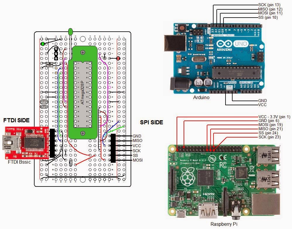
My receiver connects to my Gertboard, which, in turn, connects to my Pi. The Gertboard has the same microcontroller device as an Arduino Uno: an Atmel ATmega328P. My temperature measuring enclosure also has the same microcontroller.
My next post will tell how my data gets from the Gertboard to the Raspberry Pi. It's an interesting story and deserves a post of its own.

Asynchronous Data Transfer

I am sending data asynchronously, it can start at any time. The receiver must be able to find the start of a burst of data. For that to happen, I precede the data with a synchronization pattern. This pattern is chosen so that it can never be confused with the actual data. I accomplish this by encoding the actual data in a way that there are never more than two logic 1's or two logic 0's together. My synchronization pattern, then, must have more than two 1's and/or two 0's, together.
I use Manchester encoding with my data, which is a standard protocol. Every logic 1 in the data is replaced with a 01, while a logic 0 becomes a 10. You can see how this avoids more than two 0's or 1's together. For example: 0000 becomes 10101010. Only where there is a change in logic level will you find two 0's or 1's together. For example: 001100 becomes 101001011010.
There is a good reason for avoiding long strings of 1's or 0's: the receiver will see this an an interruption of data. The receiver has an automatic gain control, and if it sees no data, it will increase its gain to the maximum. The receiver will then output rail to rail thermal noise (See the beginning of the yellow scope trace below).
The disadvantage of this scheme is that I must transmit two bits for every single bit of data.
Here is what the start of my data looks like on the scope:
The upper trace (red) is the data to the transmitter, while the lower trace (yellow) is the received data at the Gertboard.
After every burst of transmitted data, there is a lapse of several hundred milliseconds (transmitter outputs 0V). During this time one if the temperature sensors makes its measurement and converts the measurement to two bytes of digital data. At some point during this dead time, the receiver's automatic gain control goes to its maximum. You can see the resulting noise in the beginning of the trace of the receiver's output.
You can clearly see the two synchronization pulses in both the transmitted and received data. The synchronization pulses consist of four high bits followed by four low bits. The synchronization pulses are preceded by a 101010 pattern. The receiver will recognize this pattern as actual data and will adjust its automatic gain control. There is 10 pattern following the synchronization pulses. The start of the Manchester encoded data follows that.

My Data

I am sending 20 bytes of data with each measurement:
  • byte 0: Number of sensors being accessed
  • byte 1 and 2: From the DS18B20 Scrathpad - the measured temperature
  • byte 3: From the DS18B20 Scrathpad - Upper temperature alarm. Previously set by the user
  • byte 4: From the DS18B20 Scrathpad - Lower temperature alarm. Previously set by the user
  • byte 5: From the DS18B20 Scrathpad - Resolution (9, 10, 11, or 12 bits). Previously set by the user
  • byte 6 through 17: From the ATmeta328P EEPROM - Sensor Description. Previously set by the user
  • byte 18: The number of the sensor as determined by its position in the ATmega328P's EEPROM.
  • byte 19: Cyclic Redundancy Check (CRC) byte calculated from the previous 19 bytes.
Except for byte 0, each burst of data contains the data from one temperature sensor. Each sensor is accessed, in turn, before starting with the first sensor, again.

Transmit Code

The following is a fragment of the code I usually run on my Temperature Sensor Enclosure. I say usually because I can upload other code to the box via its attached USB/FTDI port. The entire code can be seen here:
The enclosure has one permanently mounted DS18B20 temperature sensor and three receptacles for plugging in more sensors. It is possible to connect hundreds of these sensors to the enclosure (normal and parasitic power is supported). However, I only have room in the ATmega's EEPROM for the ROM codes and descriptions of 50 sensors. In the photo above, you can see I have two DS18B20 cables attached to the box. The code auto-detects the sensors when the code starts. As long as the ROM code and description of the sensor is in the EEPROM, the code will include the sensor in the measurements and in the transmitted data. If I have a new sensor, I have code to upload to the enclosure that will detect new sensors and will prompt for description, and alarm and resolution settings.
Code Fragment of Sketch Running On ATmega328P in Enclosure To Transmit Data to Gertboard.
Whenever we are ready to transmit data, the function "synchronize()" is called, followed by 20 calls to function "send_data()" - one call for each data byte in the burst. The timing is established by the global variable "bit_time". It is calculated to send data at 600 baud (1200 bps - remember it takes 2 Manchester encoded bits to send one bit of data).
Note my use of ATmega register programming rather than "bitMode" and "digitalWrite". I have a whole tutorial about register programming at by blog here:

Receive Code

The following is a fragment of code that runs on my Gertboard that receives Manchester encoded data from my Temperature Sensor Enclosure. The entire code can be found here.
Code Fragment of Sketch Running On ATmega328P on the Gertboard To Receive Data from the Temperature Sensor Enclosure.
While the transmit code is pretty easy to figure out, the receive code is interesting and bears some analysis. First, it illustrates the use of ATmega interrupts. Not shown in the code fragment are two lines in setup():
EICRA = B00000001; // Any change will trigger interrupt
EIMSK = B00000001; // Enable INT0 interrupt
This means that any change in logic level of the ATmeta328P pin connected to the receiver circuitry will trigger an interrupt. Put another way: if the logic level changes from 0 (0V) to 1 (3.3V) or from 1 (3.3V) to 0 (0V), an interrupt is issued.
Lines 18 - 20 constitutes the Interrupt Service Routine. Whenever an interrupt is issued, the variable "found_transistion" becomes true. We set "found_transistion" false, in lines 34, 41, 66, and 75. When the "while" statements in line 35, 43, 67, and 77 are reached, processing is halted until the interrupt occurs. Using the "time" and "duration" variables and the "micro()" function, the time between interrupts (corresponds to the time between transitions) can be determined.

Analyzing The Receive Data

When sychronize() is called from the main program, it looks for a positive pulse of 4 bits in duration (plus or minus 10%). It keeps looking until it find it. If it next finds a negative pulse of 4 bits in duration (plus or minus 10%), it exits the routine. It will stay in this function until it is satisfied it has found the synchronization pattern.
Once we drop out of the sychronize() function, the manchester_data() function is called. We stay in that function until 20 bytes are received. Looking at the waveform above, we start in the function at point "c". Next we look for one more transistion (lines 66 and 67) to bring us to point "d".
We look for the actual received data by entering the outer "do" loop at line 72, performing the inner "do" loop (line 74) 20 times. The logic level of each bit of data we find is tracked by the variable "present_bit". This starts as 0 because the 10 pattern following the synchronization pulses is equivalent to a Manchester code of 0.
We are at point "d" looking for the next transition which occurs at point "e". Using the threshold of 1.5 times the time of one bit (in global variable bit_time), we determine if we have encountered a change in logic level from the original 0 to a 1. Since the time from point "d" to "e" is obviously less than the threshold, we have not encountered a change in logic level. Therefore, the first bit received is a 0. The "if/else" statements in lines 80 to 86 determine the actions taken if we do exceed, or do not exceed the threshold. Since we have not, "present_bit" does not change and the variable "no_clocks" is incremented by 1.
The variable "no_clocks" has two functions. First, it indicates when we have received a bit of data. Since we must receive two bits of Manchester encoded data for each bit of sensor data, we take no action if "no_clocks" is an odd number ("if" statements lines 87 to 90). If "no_clocks" is even, we capture the last bit by shifting the contents of variable "hold_byte" to the left, and inserting the value of "present_bit" at the least significant position of "hold_byte".
The second function of "no_clocks" is to tell us when we have received an entire byte of sensor data. This will be the case if "no_clocks" reaches 16. If that is the case, the value of "hold_byte" is transferred to the next byte of the array "frame[]". When we have received all 20 bytes of "frame[]" we exit the function.
When last we were looking at the waveform, we were at point "e". We return to the beginning of the inner "do" loop to look for the next transition (point "f"). The time from "e" to "f" is also less than the threshold. We return back to the beginning of the inner do loop and find the next transition (point "f" to "g"). This time we find the threshold is exceeded so the value of "present_bit" flips to a 1 and "no_clocks" increments by 2. I think the action is easy to follow from here.

Tuesday, December 16, 2014

Jig To Load a Bootloader and Upload Sketches To ATmega328P

Note: I only write about what I know. Although there are many Arduinos and Arduino type products, I only have experience with the Arduino Uno Rev3. Likewise, the only Atmel microcontroller I know is the ATmega328P.

A Little Background (well not so little)

I have Atmel ATmega328P microcontrollers on two devices: An Arduino Uno (Rev 3), and a Gertboard. The Gertboard connects to, and is programmed by, my Raspberry Pi. In both cases the microcontroller is in a socket, so is removable. I have developed applications for both where I needed to remove the ATmega328P and install it in another device. I use the Arduino IDE system to develop sketches on both the Arduino and the Gertboard/Raspberry Pi. There is more on the Gertboard at the end of this post.
I developed a camera remote control using the Gertboard and removed the programmed ATmega chip and installed it on a circuit board. The circuit board, a 434MHz transmitter, and a motion detector were mounted in a box. I reported on that project in this blog entry.
I am completing a project that uses both the Arduino and the Gertboard/Raspberry Pi. In this case, it is the sketch developed on the Arduino that must run on an ATmega328P that is removed from the Arduino. This project, that I will report on later, requires the ability to communicate with the ATmega328P once it is installed in my mobile device.
Both projects required me to program a new ATmega328P IC. However, you can not just insert a new chip on the Arduino or Gertboard and upload sketches to it. Out of the box, the microcontroller will not use the external 16MHz crystal of the Arduino or the 12MHz resonator of the Gertboard. It will use its internal 8MHz RC oscillator frequency reference and then divide that frequency by 8. The resulting clock frequency will be 1MHz.
In order to change the clock source, you must change the logic level of a couple of "fuse" bits. I use "" around the word fuse, because the term is actually a carryover from the time when ICs, like microcontrollers, had actual fuses. Each fuse would control the logic level of one bit. If the fuse was blown, the bit would be a 0, if not blown it would be a 1. You could always change a 1 to a 0, by blowing the fuse, but you had no way to change a 0 to a 1. If you wanted a 1, but programmed a 0, in error, you had to replace the chip. That is not the case today.
Now, "fuse" bits can be changed from 1 to 0 and 0 to 1 anytime. The ATmega328P has three, eight bit bytes of these "fuse" bits. They control different functions and leave the factory in a default configuration. In addition, there is a byte (8 bits) of lock bits. More on these later. To setup a new ATmega328P for the Gertboard, you run a program on the Raspberry Pi called avrsetup. All this program does is to use avrdude to set the lock bits and the fuse bits. It leaves all bits not concerned with the clock frequency to their default settings. The four bits that select the clock source are changed from "Calibrated RC Internal Oscillator" to "Full Swing Crystal Oscillator". And, the divide by 8 function is turned off. Avrdude is like an operating system for the Atmel microcontrollers. All programming of the microcontrollers are done through avrdude even if you use the Arduino IDE.
For the Gertboard/Raspberry Pi, setting those fuse bits is all you have to do to use a new ATmetga328P. That is not the case with the Arduino. A new ATmega328P for the Arduino needs those same fuse bit changes and needs one more thing: a bootloader installed. What is a bootloader, and why doesn't the Gertboard need one?
When you upload a sketch to the flash memory of the ATmega328P, there are two direct ways. One is to use a parallel configuration, which I will not mention further (just going to forget it exists). The other is to use the chip's SPI (Serial Peripheral Interface) bus. This synchronous, serial, bus consists of four lines: SCK (Serial Clock), SS (Slave Select), MOSI (Master Out Slave In), and MISO (Master In Slave Out). I upload sketches to the Gertboard via the SPI bus. The Raspberry Pi is the Master, the ATmega328P on the Gertboard is the Slave. Since the direct programming method is employed, no bootloader is necessary.
Atmel, in their wisdom, realized that not everyone would like to use the SPI bus, but would wish to use the more universal serial bus (or something else). The serial bus interface has several names such as RS232 and UART. It consists of several signals: TX (transmitted data) and RX (received data). The TX of the one device is connected to the RX of the other device, and RX of the first device is connected to TX of the second device. There are more signals, but, typically, they are not used. However, a signal, DTR (data terminal ready), for example, may be used to reset the ATmega328P. Once the ATmega328P is reset, it will start running any sketch loaded in flash from its beginning.
Atmel provided an area of flash memory for the user to install code allowing the rest of the flash memory to be uploaded via the serial bus. This code is the bootloader. For the ATmega328P, it can take up as much as 2 Kbytes of the 32 Kbytes of flash memory. The flash memory, not reserved for the bootloader, is the Application memory. Once the bootloader is loaded, it can load a new sketch into the Application memory via the RX and TX connections of the serial bus.
So, how do you get the bootloader loaded in a new ATmega328P? It requires hardware and software. Since a new ATmega328P has no bootloader, the bootloader must be installed from the SPI bus - the direct, primary, interface to the chip. That means you need an in-circuit programmer. There are inexpensive, commercial, units available like the USBtinyISP. They have USB on one end and the four SPI connections on the other end (SCK, SS, MOSI, and MISO), plus power and ground. They have a 6 pin ribbon cable and connector that plugs into your target device that contains the microcontroller chip you want to access. There is a standard 6 pin SPI configuration that receives the ribbon cable connector. My Arduino Uno has two of these 6 pin connectors, one for the ATmega16U2 and the other for the ATmega328P. You can install a new ATmega328P on your Arduino Uno and connect a programmer to it to upload the bootloader. But, I don't do that.
I have no experience with the aforementioned programmers so I will not discuss them. There is another programmer that works really well - and I have experience with that one. This programmer is the Arduino itself. You can't use it to load a bootloader on its own ATmega328P, but it can be used to install a bootloader on another Arduino's ATmega328P. However, I do a variation of that. I use the Arduino Uno to install the bootloader on an ATmega328P that is on a jig I made. This is the jig that is the subject of this blog post.
Now we need some software. There are two pieces of this. One piece is the bootloader itself. The Arduino IDE package has copies of the bootloaders. There are different bootloaders for the different ATmega devices and the different Arduinos. The other piece of software is the software to load the bootloader. This software is a sketch running on my Arduino Uno that is used as a programmer. This software must do several things. I have not studied this software to know how it works, but from my knowledge of the ATmega328P, I know it must do the following:
  • Program the fuse bits to select the clock source to "Full Swing Crystal Oscillator" and turn off the clock divide by 8.
  • Set the Lock bits to allow programming of the bootloader in the Boot Flash Section
  • Set the fuse bits to the amount of flash memory devoted to the Boot Flash Section (up to 2 KBytes)
  • Upload the bootloader program to the Boot Flash Section
  • Set the lock bits so the Boot Flash Section can no longer be written to, protecting it from being overwritten.
There is one last point to consider before moving on to the details of my programming jig. Could there be an Arduino that programs the microcontroller directly over the SPI bus? Certainly. There are ICs that convert USB to SPI. That would eliminate the bootloader. We are forgetting one thing though: How do you communicate with a sketch? For example, a sketch that requires you to answer some questions before proceeding. The answer is the Serial Monitor. Access to the Serial Monitor is via the same interface the Arduino uses to upload sketchs - the same TX and RX connections to the ATmega328P.
For the Gertboard, the Serial Monitor button exists on the Arduino IDE running on the Raspberry Pi. However, it does not work. A separate connection to the ATmega328P's UART must be made. Consequently, the Raspberry Pi/Gertboard requires six signal connections: SCK, MOSI, MISO, SS, and TX and RX. The Arduino UNO only has two ATmega328P signal connections: TX and RX. For the Gertboard, I have to open a separate terminal window and run a terminal program to communicate with a running sketch. All-in-all, the loss of a little flash memory to the bootloader seems worthwhile.

An ATmega328P Programming Jig

The following is the schematics and board layout diagram for my jig:
Schematics For ATmega328P Programmer
Here is the layout of the board with components and wiring:
Board Layout For The ATmega328P Programmer
Looking at the board layout, the ATmega328P sits in a 28 pin ZIF socket (all that green in the diagram). This allows an IC to be quickly inserted and removed. Check out the product page from Sparkfun.
The connector pins labeled SPI are for female - female jumper wires. This interface connects to the Raspberry Pi or to the Arduino Uno. Connections to the Raspberry Pi are to set the fusebits on an ATmega328P, and to load sketches developed on the Gertboard. The connections to the Arduino UNO are only to install a bootloader on an ATmega328P.
Note the interface labeled "FTDI". This interface is used to upload sketches to an ATmega328P (must have the bootloader installed) that I have developed on my Arduino. In addition, it provides access to the Arduino IDE Serial Monitor, allowing us to communicate with a program running on the jig's ATmega328P. FTDI is the name of a chip manufacturer that makes USB to Serial ICs. The FTDI interface on my jig connects to a Sparkfun FTDI Basic breakout board. This small board has a mini USB on one end and a six pin female connector on the other that plugs directly onto my jig.
There is a three pin female connector labeled resonator. Since the Gertboard and the Arduino Uno operate on different frequencies, the connector allows a 12MHz resonator to be connected for the Gertboard sketches and a 16MHz resonator for the Arduino operations.
There are two LEDs on the jig. The green one lights whenever power is applied to the jig. 5V can come from the FTDI board or the Arduino Uno. The Gertboard will supply 3.3V. The red LED is a sanity check and is connected to PB1 of the jig (this corresponds to pin 9 of the Arduino). After loading a bootloader, I can check if I can upload a sketch to a new ATmega528P by running a version of Blink. Anytime I need to check the jig or my connections, I can program that red LED.

Parts List

  • Prototype Breadboard PCB, half size: Adafruit 1609, $4.50
  • ZIP Socket, 28 pin: Sparkfun PRT-09175, $2.95
  • Right Angle Header Strip for FTDI and SPI: Mouser 571-9-103323-0, $2.24 for a strip of 40 pins
  • ATmega328P Microcontroller: Mouser 556-ATmega329K-PU, $3.55
  • Socket strip for Resonators: Digikey 1212-1125-ND, $3.89 for a strip of 64. Perfect socket for resonator pins
  • 16 MHz Resonator: Mouser 520-ZTT1600MX, $0.50
  • 12 MHz Resonator: Mouser 520-ZTT1200MX, $0.50
  • Red LED - clear housing: Digikey C503B-RCN-CW0Z0AA1-ND, $0.15
  • Red Green - clear housing: Digikey C503B-GCS-CY0C0791-ND, $0.24
  • 10μF, 16V Tantalum capacitor: Mouser 581-TAP106K016CRW, $0.53
  • 0.1μF 100V Ceramic capacitor: Mouser 1C20X7R104K100B, $0.18 ea.
  • 1N4148 diode: Mouser 512-1N4148, $0.10
  • 10KΩ Metal Film Resistor: Mouser 71-RN55D-F-10K, $0.10
  • 1KΩ Metal Film Resistor: Mouser 71-RN55D1001F/R, $0.10 ea.
I use LEDs with clear bodies. I anticipate using LEDs in battery powered projects so I want to minimize the current consumed by LEDs. Normally, you calculate the series resistor to deliver about 10ma. of current to drive the LED on. A resistor of about 330Ω is commonly used. The LEDs with the clear housings require much less current so I typically use a 1KΩ series resistor (about 2ma.). Even that can seem too bright, I might try 2KΩ on my next project.

Using the Jig

Diagram used for all situations follows:
Connecting The Programming Jig

Installing a Bootloader

Make connections as in the diagram above from the jig's SPI connector to the Arduino. Make sure there is a 16MHz resonator installed on the jig. Install an ATmega328P on the fixture. By the way, I probably should have mentioned it before, but do NOT use a ATmega328 unless you are capable of adding support for the device in avrdude and the Arduino IDE. The two devices have different signatures so the ATmega328 will not be recognized unless you are capable and willing to make the software changes I mentioned. The two devices are about the same but the "P" version runs at lower power.
Do the following from the Arduino IDE:
  1. Upload the sketch ArduinoISP: Files\Examples\ArduinoISP.
  2. Select the Arduino Uno board (selects the bootloader for the ATmega328P because that is the microprocessor for the Uno): Tools\Board\Arduino Uno.
  3. Select the Arduino as ISP as the programmer: Tools\Programmer\Arduino as ISP.
  4. Install the bootloader: Tools\Burn Bootloader.
That's all there is to it. It takes less than a minute for the process to complete. Once the TX and RX LEDs, on the Arduino, stop blinking, the bootloader is loaded.

Uploading Sketch Via FTDI

Once the boatloader is installed, you can upload a sketch to the jig using the FTDI Basic board. When I plugged my FTDI Basic into my USB port, for the first time, I found that the drivers had already been installed on my Windows 8.1 system. They must have been part of the Arduino IDE installation. If you do not have the drivers, check out Sparkfun's product page for instructions on getting them. The FTDI Basic costs about $15 at Sparkfun.

Raspberry Pi/Gertboard

The Gertboard is a expansion board that connects to the Raspberry Pi's GPIO pins. It has several different circuits useful for interfacing the Raspberry Pi to the outside world. The Gertboard works with all thee versions of the Raspberry Pi (A, B, B+). Here is what the Gertboard offers:
  • ULN2808 containing six open collector outputs, each capable of driving a 500ma. load up to 50V (from a separate power source)
  • MCP4802 dual channel D>A (digital to analog) converter
  • MCP3002 dual channel A>D (analog to digital) converter
  • ROHM BD6222HFP H bridge motor controller (need a separate power source)
  • 12 output buffer circuits
  • 12 input buffer circuits
  • 12 red LEDs
  • 3 momentary switches
  • ATmega328P microcontroller. Running on 3.3V with a 12MHz resonator. All IO pins are available.
The documentation, unbelievably not provided when you purchase the product, is excellent. It can be found here. The manual references C and python programs that can be used to test out each section of the Gertboard. In order to use the ATmega328P, a bit of software must be loaded in the Raspberry Pi. This is also referenced in the manual and is available from Gordon Henderson. Here is a link to his blog. It all just works great. Newark Element14 has the Gertboard for $40. Inexplicably, Sparkfun sells it for $60. On Sparkfun's product page it lists the microcontroller as an ATmega328. It's an ATmega328P.
My jig will look to the Raspberry Pi just like the ARmega328P on the Gertboard. Therefore, if you want to interface an ATmega328P to a Raspberry Pi without using the Gertboard, the same software from Gordon will do the job. Just make the connections as in the diagram above.
Once you upload a sketch, you may need to communicate with the ATmega328P, such as you do with an Arduino. For the Arduino, you use the Serial Monitor function of the Arduyino IDE. You will not be able to do that from the Raspberry Pi, but you can still communicate with the ATmega328P. You connect RX and TX on the FTDI side of the jig to TX and RX, respectively, on the Raspberry Pi. You connect the FTDI TX to pin 10 (RX) of the Pi and FTDI RX to pin 8 (TX) of the Pi. The alternative to the Serial Monitor is to use a terminal program like minicom within a terminal window on the Raspberry Pi. The installation and use of the minicom program is covered in the Gertboard User's Manual.

Going On From Here

Obviously, the jig as it stands, does not have much utility as it only uses one of the many ATmega328P's IO pins. However, the concept can be used to make something more useful. Here is an example of a project in the works:
All of this goes into an enclosure. I will add temperature sensors and a RF transmitter, with antenna. The ATmega328P is mounted in a standard 28 pin socket instead of the Zif socket. A 16MHz crystal provides the clock reference.
Note the FTDI basic board. It's used to communicate with the ATmega328P. This is necessary to tell the LCD what text to display. Once power is applied, the display is blank. I attach the FTDI Basic board, connect it to the PC, via a USB cable, and bring up the Arduino IDE. The sketch is already running on the ATmega328P so I click on the Serial Monitor and am greeted with a request to type a message. Once that is done, the message is displayed in a Time Square Scroll. I can then remove the FTDI Basic board.
Please check out my blog entries of March 7, 2013 to April 18, 2013 for discussions of my LCD projects for the Raspberry Pi. The last two posts, specifically, are about my Times Square Scroll software. I have since converted the software from python to C to run on the Arduino. I'll report on that effort at a later time.

Sunday, July 13, 2014

Cyclic Redundancy Check (CRC) of DS18B20 Serial Data

This is a continuation of my last three blog posts.
Maxim has application note 27, "Understanding and Using Cyclic Redundancy Checks with Maxim 1-Wire and iButton Products", that I will refer to here. You can see this here.
If you transmit data from one place to another you want to know that the data arrived unchanged. The cyclic redundancy check is the best way to tell you if the transmission was successful.
We transmit serial data from two sources within the DS18B20: from its Read Only Memory which has the ROM code stored, and from the scratchpad memory. Basically, while transferring data to us, the user, the DS18B20 looks at the data it is sending, one bit at a time, and makes a calculation. The result of that calculation is an additional byte that is tacked on to the data stream. The value of this byte depends solely on the bits that have preceded it in the transmission. This additional byte is the CRC byte. The ROM code is actually 7 bytes long but the CRC byte makes it 8 bytes long. The scratchpad data is 8 bytes long and its CRS makes it 9 bytes long.
My code calculates the CRC as each bit of each byte is received. One of the nice things about CRC, and, this should be kept in mind, is if the transmission was successfully received, my calculation of the CRC will be 0. It's very easy to check for 0 in code. Any result besides 0 means the transmission failed.
How do you calculate CRC? It's hard to put that into words. The mechanism for calculating CRC is generally expressed as an electronic circuit. You can actually build this circuit and calculate the CRC, or you can emulate this circuit in software. I have done the latter in my One_wire_DS18B20 library file. I was surprised how few lines of code it took to write the CRC function. More on this later.

Getting Into Electronic Hardware

Here we go diving into interesting waters. But, I don't know how to otherwise discuss how this all works. So here we go. Maxim gives a representation of the electronic circuit in it's figure 2 of the application note. Here it is:
I have my own version of that figure that shows more detail, especially what is in those boxes called stages:
There are two different kinds of parts here, the boxes are called flip-flops (No connection to the ones you wear to the beach). Let's look at a flip-flop a little more closely:
Why the funny name, flip-flop? The name describes the functionality, perfectly. The output from the part can be made to flip from one state to another. That is, from a high voltage to a low voltage; or, stated another way, from a logic HIGH state to a logic LOW state; or, stated yet another way, from a "1" to a "0". Of course going back in the other direction is just as easy. Flip-flops make up a large part of the circuitry in your computer microprocessor. There are thousands of them. The simplest can be constructed with just two transistors. The flip-flip we are showing here is a bit more complex and is called a D flip-flop. Below the flip-flop, is a timing diagram that plots voltage (vertical) against time (horizontal). When the voltage is at it's high state we call this a logic "1". When the voltage is near 0 volts, we call this a "0". (That is arbitrary, we could call a high voltage a "0" and a low voltage a "1").
We see three signals, or waveforms: "Data", "Clock", and "Output" (we are going to ignore reset). "Data" is the information that is being transmitted serially, one bit at a time. "Clock" is another signal, and when it makes a transition from a "0" to a "1", the logic level the device sees on its "D" pin, will appear at its "Q" pin. We show that the data on the "D" pin is "latched" on the rising edge of "Clock" by those upward arrows on the "Clock" waveform. The first time we see "Clock" going from a low to a high, the "Data" happens to be high (or a "1"). After a really short delay, that "1" appears at the output of the flip-flop. That little delay is important. It is not obvious why here, but will be when we consider more than one flip-flop. If you look at each rising transition you will see the output will mirror what is at the "D" pin. So far, not so interesting. But. wait, let's connect a second flip-flop to the first one.
We connect a second D flip-flop so that its "D" ("D" for data, by the way) pin connects to "Q" of the first one. "Clock" connects to both flip-flops. Now we can see why that little delay is important. When we look at the second time the "Clock" goes from low to high, we see that the "D" pin of the first flip-flop is low, so the output of the first flip-flop wants to go low to follow the input. However, there is a slight delay so it stays high for a little while longer. If that delay was not there, the output of the first flip-flop would be changing at the exact time that "Clock" is latching the data at the input of the second flip-flop. What would the output of the second flip-flop be? A "1" or a "0"? Who knows! That little set-up delay assures that the input of the second flip-flop is a "1" long enough so the "Clock" latches a "1" at the output of the second flip-flop.
Is this circuit any more useful than the first? The usefulness of the circuit will be evident if we add more flip-flops. Let's have a total of 8:
Remember, "Data" is the information coming into the circuit one bit at a time. "Clock" captures that information in the first flit-flop. As new bits arrive, they cascade to the other flip-flops from left to right. Each rising edge of "Clock" shifts the information on "Data" from flip-flop to flip-flop. Thus, this circuit is called a shift register. The flip-flop outputs are labeled "Q7" - "Q0".
The circuit is also called a serial to parallel converter. After shifting in the serial data enough times to get the first bit cascaded down to the last flip-flop, the original eight bit data word is available on "Q7" - "Q0" in parallel format. We could connect "Q7" - "Q0" to other circuitry if we wished.
Why the grayed out areas? We don't have enough information to know if the logic levels in these areas are a "1" or a "0".
My project emulates the shift register in software. Every time we ask for data from the DS18B20, we call on a couple of functions in my 1_Wire library. We emulate "clock" with a "for" loop to shift in each bit of each byte. The "Q7" - "Q0" outputs are represented by an eight bit variable. We call that loop enough times to capture each byte in the message from the DS18B20.
As we shift in each bit, we do a calculation to determine the CRC value. We continue that calculation until the last bit of the last byte of the message has been shifted in from the DS18B20. For example, if we were capturing ROM code, we would capture eight bytes. The last byte of the ROM code is the CRC value (calculated by Maxim). After shifting in all 64 bits, the result of our calculation should be "00000000" (Recall my forth paragraph above).

Enough Background - Getting To The Cyclic Redundancy Check

Let's repeat that figure at the top of this post:
Notice that this is similar to the shift register above. We have added three parts called exclusive OR gates. They each have two inputs on the left and one output on the right. The exclusive OR is one of a series of logic circuits. Some of the others are inverters (also called NOT gates), AND gates, and OR gates. These devices look at the logic levels at their inputs ("1" or "0") and decide what the logic level of their output will be. The output of the inverter is opposite of the input. The output of the AND gate is "0" unless all the inputs are "1". The output of the OR gate is a "1" if any of it's inputs are "1". The output of the exclusive OR gate will be "0" if the logic level of the inputs are the same (both "0" or both "1"). If the inputs are different ("0", "1" or "1", "0") the output will be a "1".
That CRC circuit seems to be a bastardized version of the shift register. The output from the last stage is fed back into the circuit. This circuit is specific to the way Maxim handles the CRC for devices that transfer data in eight bit bytes. They have a different circuit for devices that transfer 16 bit bytes. That circuit has 16 "stages"
The type of CRC circuit is also know by its polynomial, a mathematical expression representing the number of stages, and where, and, how many exclusive ORs are in the circuit. The polynomial for our circuit is shown on the figure above from Maxim's application. It is X8 + X5 + X4 + 1. This means we take the output of the forth, fifth, and eighth stage as inputs to our exclusive OR gates. There are other schemes with different number of exclusive OR gates that feedback to different stages. These have different polynomials.
The mathematics of the cycle redundancy check is quite involved and I won't begin to discuss it here. There is plenty of in-depth information on the web. Let's move on to the final discussion of implementing the CRC in software.

Calculating the CRC in Software and in Our Equivalent Circuit

The following code is taken from my calculateCRC_byte function found in my One-Wire_DS18B20 library.
The Equivalent CRC Circuit diagram contains the value of the CRC in the eight bits of "Q7" - "Q0". Note, however, the sketch variable "CRC" is an int, not a byte, making it 16 bits long. The reason "CRC" is 16 bits long is due to lines 11 and 14 of the sketch. On those lines, "CRC" is operated upon by a value that is nine bits long. Hence, "CRC" must be longer than 8 bits. When we reach the bottom of the function, the top eight bits of "CRC" will always be "00000000". The lower eight bits will be equivalent to "Q7" - "Q0" in the circuit. The top eight bits will also be "00000000" when we arrive at the "IF" statement in line 10.
The sketch has two loops, an outer loop for the number of bytes we send to the function, and an inner loop that runs eight times, once for each bit of the incoming byte, "inByte[i]".

Lines 9 Through 15 of the Code

Comparing the equivalent circuit to the sketch, the "IF" statement in line 10 implements, exactly, the exclusive OR gate on the left of the equivalent circuit. Let's look at that statement closely:
"if ((CRC % 2) ^ (inByte[i] % 2)){"
The "%" operator is called a modulo. The result of the modulo operation is the remainder after dividing whatever is to the left of the operator by whatever is to the right of the operator. In this case, we divide the current value of the variable "CRC" by 2. If the value of the variable "CRC" is even, the modulo will be "0". If odd, the module will be "1". Whether or not "CRC" is even or odd depends solely upon the value of its least significant bit (last bit on the right). Therefore, the value of "CRC % 2" is the value of the least significant bit of "CRC".
The CRC Equivalent Circuit holds the value of the CRC on its outputs "Q7" - "Q0". Applying the same argument as in the last paragraph, "CRC % 2" is the value of "Q0", the least significant bit of the CRC stored in the flip-flops.
Using what we learned above, "inByte[i] % 2", will give us the value of the least significant bit of the data byte, "inByte[i]". This is exactly the same as the current value of "Data" in the CRC Equivalent Circuit.
The symbol "^", in the "IF" statement, sitting between the two modulo expressions, is the bitwise exclusive OR operator. Because, "Q0" and "Data" connect to the exclusive OR at the left of the equivalent circuit, the entire "IF" statement is equivalent to that same exclusive OR gate. The result of the "IF" statement is precisely the same as the output of the left-hand exclusive OR gate. From our discussion of how the exclusive OR works, if the value of the least significant bit of the variable "CRC" and the value of the least significant bit of the array "inByte[i]" are the same (both "0" or both "1"), the result of the "IF" statement will be "0", otherwise (one is a "0" and the other a "1") the result will be a "1". In the same manner, if the value of "Q0" and the value of "Data" are the same, the output of the exclusive OR gate in the equivalent circuit will be "0". If different, the value will be "1". This output is the input to the first flip-flop at the left of the circuit, and one of the inputs of the other two exclusive OR gates in the equivalent circuit.
We described of the exclusive OR gate as being a "0" if its inputs were the same and a "1" if they were different. We used that description to evaluate the "IF" statement and the output of the exclusive OR at the left of the equivalent circuit. There is another useful way to look at an exclusive OR gate, and we will use that way in the following discussion. We can look at one input of an exclusive OR as a control input that controls the relationship between the second input and the output of the gate. If this control input is a "0", the output of the exclusive OR will follow the other input. If the control is a "1", the output will be opposite of the input (A "0" becomes a "1" and a "1" becomes a "0").
The result of the "IF" statement controls which of the two operations we apply to the value of "CRC" (either line 11 or line 14). We either exclusive OR "CRC" with "100011000" or "000000000". In our new way to look at the exclusive OR gate, those two series of nine bits are the control inputs to nine exclusive OR gates. They control what happens to value of the variable "CRC" at that point in the sketch. We can call them a control word.
Let's operate on a sample byte to see what those control bits do:
011010101 Sample 011010101
000000000 Control Word 100011000
011010101 Result 111001101
Note that when the control word is "000000000", there is no change to the sample, the result is the same as the sample.
I said the nine bit control word was like having nine exclusive ORs. But, six of those bits are always "0", both in line 11 and line 14. Consequently, we can replace those six exclusive ORs with direct connections, meaning there are only three exclusive ORs. This happens to be the same number of exclusive OR gates in our equivalent circuit. In fact, they are in the same relative positions. The most significant bit of our control word corresponds to the left-hand exclusive OR gate. The two bits of the control word that can change, are in exactly the same place as the other two exclusive OR gates in the circuit.
The purpose of the exclusive ORs are to modify the value of CRC existing at "Q7" - "Q0", or the value of the variable "CRC", before there is further processing. If the control word is "000000000", there will be no change in the value of "CRC". Since, the effect of exclusive ORing "CRC" with "000000000" is no effect at all, lines 13 - 15 of the sketch are superfluous. They do not appear in my actual code. I only added them here because it made explanations easier.
Let's look at the output of our exclusive ORs, be they in the sketch or the equivalent circuit. Exclusive ORing with "000000000" was the result of the output of the "IF" statement being "0". Let's see what happens to the equivalent circuit when the output of the left-hand exclusive OR is "0". First, the input to the left-hand flip-flop will be "0". The output of the left-hand exclusive OR also connects to an input of the other two exclusive ORs. Let's consider the output of the left-hand exclusive OR to be the control input to the other two flip-flops. If this control input is "0", the output of the two flip-flops ("Q4" and "Q3") will be the same as their other inputs, meaning there will be no change to the CRC.
When the output of the "IF" statement is "1" we will modify the value of the variable "CRC" with "100011000". At the equivalent circuit, the output of the left-hand exclusive OR will be a "1". The effect will be that the input of the left-hand flip-flop will be "1" and the control input to the other two exclusive ORs will be a "1". This will cause the "X4" to be of the opposite logic level of "Q4" and "X3" to be of the opposite logic level of "Q3". In other words, we have flipped those two bits.

Lines 16 and 17 of the Code

"Whew", we now have the variable "CRC", and the inputs of those flip-flops, set up for the next operation.
In the equivalent circuit, the signal labeled "Clock", which has been at "0" will briefly go to a "1" and back to "0". As in our discussion of the shift register, the logic level at the inputs of those flip-flops will now appear at the outputs of the flip-flops. This has the effect of shifting the current value of CRC down one position. Sometime after that, the value of "Data" will have the next bit of the serial data coming into the circuit.
Our sketch has an exact equivalent to the "clock" signal. That equivalent is line 16: "CRC >>= 1;". This operation will take the value of "CRC" and shift all 16 bits down one bit position to the right. A "0" will be shifted into the most significant bit of "CRC".
The next line, line 17, shifts the eight bits of "inByte[i]"down one bit to the right. A "0" will be shifted into the most significant bit. The operations of lines 16 and 17, are directly comparable to applying the clock to the flip-flops, and introducing the next data bit, in the equivalent circuit.

An Example

Let's take an example of two bytes and walk them through the sketch. Let's assume the two bytes are "10110100" and "01010011". If I run "10110100" through the sketch, by itself, the resulting CRC will be "0000000001010011". If we ignore the top 8 bits, the CRC is the same as the second byte we will pass to the sketch. Since the second byte is the same as the CRC of the first byte, the final CRC should be "0000000000000000", after processing both bytes.
First Byte 1:
i j inByte[i] CRC CRC Before Right Shift
0 0 10110100 0000000000000000 0000000000000000
0 1 01011010 0000000000000000 0000000000000000
0 2 00101101 0000000000000000 0000000100011000
0 3 00010110 0000000010001100 0000000010001100
0 4 00001011 0000000001000110 0000000101011110
0 5 00000101 0000000010101111 0000000010101111
0 6 00000010 0000000001010111 0000000101001111
0 7 00000001 0000000010100111 0000000010100111
0 7 00000000 0000000001010011 <-After the Final Shift
Now Byte 2:
i j inByte[i] CRC CRC Before Right Shift
1 0 01010011 0000000001010011 0000000001010011
1 1 00101001 0000000000101001 0000000000101001
1 2 00010100 0000000000010100 0000000000010100
1 3 00001010 0000000000001010 0000000000001010
1 4 00000101 0000000000000101 0000000000000101
1 5 00000010 0000000000000010 0000000000000010
1 6 00000001 0000000000000001 0000000000000001
1 7 00000000 0000000000000000 0000000000000000
1 7 00000000 0000000000000000 <-After the Final Shift
The DS18B20 transmits data least significant bit first. If you had an application that transmits most bit significant first you would have to modify the "IF" statement. Assuming the data coming in is 8 bits in length, you could replace "inByte[i] % 2", with "inByte[i] > 127". Also, "inByte[i] >>= 1" would be replaced with "inByte[i] <<= 1". If the CRC is calculated using a different polynomial, you would have to modify line 11 accordingly.
Feel free to download and experiment with this sketch. You can enter as many bytes as you wish. Just add some print statements and setup() and loop() to feed the function.

Monday, July 7, 2014

DS18B20 Connected Using Parasitic Power

This is a continuation of my last two blog posts.

Parasitic Power and 1-Wire Devices

The 1-Wire devices have three pins, one for power, one for ground, and one for data. However, it is possible to connect the device without connecting to a source of power. In that case, both the ground and power pins are connected to ground. That simplifies cabling as it is only necessary to run two wires instead of three. A device connected in this matter is said to be connected using parasitic power. The device gets its power, parasitically, from the data line. And, the data line is powered through a 4.7K pull-up resistor to the power source (5V for the Arduino). That relatively high value of resistance still allows the Arduino or a DS18B20 to pull the data line to a low logic state (near ground). That arrangement is sufficient to power the device for all operations except when the device is undergoing temperature conversion and when writing from the scratchpad to the device's EEPROM (not the ATmega EEPROM). For those operations, the device may draw as much as 1.5mA. That's not a lot of current, but still more than can be supplied through that pull-up resistor. For those two operations, we connect the data line, directly, to the power source. Of course, once we do that, we can't have any other operation going on that requires a transfer of data in either direction (can't pull the data line low).

Parasitic Power Control Circuit

Obviously, we need a switch to control when we connect the data line to the power source. The switch I devised can be seen in the figure below:
My switch is the 2N5087 PNP transistor. Why that transistor? I just happened to have a couple. The transistor can supply about 100ma., so more than 67 parasitically connected devices could sit on the bus. Sparfun has a 2N3906 which should work just as well. Actually, this one will sink 200ma. If you are interested, Sparkfun has a tutorial about how transistors operate. Look here.
Once a low voltage (near 0) is applied through the 1K resistor to the base of the transistor, the transistor "turns on" making a near short circuit between the collector (connected to the power source) and the emitter (connected to the the data line). I use an Arduino pin to control the transistor (PB1 in my case). When I want the switch to be off, I program PB1 to be an input. As an input, the Arduino can not supply any current to the transistor's base-emitter junction so the transistor can not turn on. When I want the switch on, I program the logic level at PB1 to be LOW and program the pin to be an output.

Detecting Devices Connected Using Parasitic Power

It is not necessary to keep track of the devices that are connected using parasitic power. You can use the library function command read_power_supply(). Like all function commands it must be preceded by initialization(), and either match_rom() or skip_rom(). Function match_rom() will address only one device - the one with the ROM code you pass to it. If that device is connected with parasitic power it will pull the data line low. If skip_rom() is employed, ANY device connected with parasitic power will pull the data line low.

Programming Consequences of Devices Connected Using Parasitic Power

In my library function Convert_t(), if a device is not connected using parasitic power, I let the device inform my code when the convert operation is complete. The device will pull the data line to a logic LOW while the conversion is taking place. My library function reads the data line every millisecond. When a logic HIGH is read my code can move on and do its next operation. According to the data sheet, the resolution at 12 bits should take no more than 750ms. I found that the conversion is done in about 550ms. at 12 bit resolution.
If using parasitic power, the device can not pull the data line low because of the hard pull-up. The only option is to pass the resolution to the convert_t() function and use a delay() statement to give the device enough time to make the conversion. To be sure enough time is given, I use the specification in the data sheet.
You can look at my Read_Temperature.ino sketch to see more of my implementation of parasitic power. It is one of my files on GitHub, but you can see it here.

Saturday, July 5, 2014

My 1-Wire Arduino Library for DS18B20 Temperature Sensor

This is a continuation of my last blog post.

The Include File For the 1-Wire DS18B20 Library

This 1-wire library will work equally well with an Arduino and a Gertboard.
At the top of the file are #define statements to account for your hardware set-up. Unless you use the same hardware choices I made, you make the appropriate changes to the file and save the file.
The first #define is for CLOCK_FACTOR. I reported in an earlier post that the delayMicroseconds(), Arduino IDE, function is not accurate when using the Gertboard. I tested this thoroughly, at different values, using an oscilloscope. My results show that you must divide the desired delay by 0.67 to get an accurate delay. Consequently, if you use the Gertboard, make the clock_factor 0.67. Select 1.0 for the Arduino. The difference is caused by the 12MHz clock frequency of the Gertboard compared to 16MHz of the Arduino. The delay() function requires no correction.
The rest of the #defines relate to the selection of the two Arduino data pins you select. One pin is the data pin for the 1-wire bus, and the other is the pin that controls the transistor for parasitic power. I will have a post devoted to the parasitic power transistor circuit. Hopefully, my comments, in the file, are enough to guide you through the selections.
If you use the Gertboard you can take the pin names as they appear by the J28 connector (PB1 for example). These are the same designations as used in the ATmega's data sheet, and, more importantly, the same designation as used in the avr/io.h include file. If you use the Arduino, where pin numbers are 0 to 13, you will need to convert them to the ATmega numbers.
Arduino ATmega Arduino Atmega Arduino Atmega
0 PD0 5 PD5 10 PB2
1 PD1 6 PD6 11 PB3
2 PD2 7 PD7 12 PB4
3 PD3 8 PB0 13 PB5
4 PD4 9 PB1
The rest of the file declares the functions in the library source file. These are the public functions, those that can be called from a sketch, and the private functions, those that are not available from sketches.

The Soruce File For the 1-Wire DS18B20 Library

Most of the functions are short. Their comments are longer than the code. You will have to be familiar with ATmega register programming and bit manipulation. I have tutorial on useing direct register programming here.
In the next several posts, I'll go into some detail on the search_device() and calculateCRC_byte() functions. But, first, I need to address parasitic power and what to do about it. That's next.

Wednesday, February 12, 2014

Gertboard - Creating Delay Function With Timer/Counter

My last blog post mentioned that the Arduino built-in delayMicroseconds() function was very inaccurate. The error was a whopping 50% when measured with an oscilloscope. As I wanted to investigate some of the intricacies of the ATmega328P registers I thought to write my own delay function.

Counter - Timer Features of the ATmega328P

There is tons of information on the web about using the ATmega timer/counters so the following will be a bit sketchy. The datasheet is a must to have available when talking about the ATmega functions. However, the datasheet is rather terse so sometimes you have to read between the lines, experiment like I am doing, or read of someone else's experience like you are doing here.
There are three timer/counters on the chip: 0, 1, and 2, They all have somewhat different features. Timer/counter 0, and 2, are eight bit counters so can only count up to a maximum of 255 (28). Timer/counter 1, has a 16 bit counter so can count up to 65535 (216).
Timer/counters 0 and 2 are almost identical. It seems that the intended use for timer/counter 2 is as a real-time clock. It kind of assumes that a 32 kHz watch crystal is connected to pin TOSC1. However, on the Gertboard, and most Arduinos (as far as I know) The 12 or 16 MHz resonator is already connected to that pin. Timer/counter 2 does have six prescaler (clock divider) selections while 0. and 1 have five.
Timer/counter 0 and 2, with their eight bit counters are well suited for controlling motors by pulse width modulation (PWM) while timer/counter 1 is best for servos and things my delay project. Timer/counter 0 and 2 have four modes of operation, a "Normal" mode, a "Clear Timer On Compare Match Mode" (CTC), and two pulse width modulator modes. Timer/counter 1 has all the modes of the other two with an additional PWM mode.
In all but two of the modes, the counters in the timer/counter circuit count up with each clock pulse received. When it reaches either its maximum value (255 or 65535), or a value you program, it starts over from zero. For pulse width modulation, you use the counter to establish a period of time. But, that only gives you half of what is necessary to control motor speed. For each time period, you need to control the percentage of time that you provide voltage to your motor. To provide that functionality, each timer/counter has two comparators (8 bit for 0 and 2, and 16 bits for timer/counter 1). You program a value into a comparator and when the count in the counter matches that value, the state of the I/O pin associated with the Timer/counter/comparator changes. When the counter reaches it's top value and returns to zero, the state of the I/O pin changes again. This results in two changes of state in each counter cycle (OFF to ON, and ON to OFF or ON to OFF, and OFF to ON). There are two modes where the counter counts down as well as up. Here, the state of the I/O pin changes when the counter count matches the comparator while counting up to its maximum value and matches it again on its way down to zero.
Since there are two comparators, each timer/counter can control two I/O pins. You can control two motors or two servos from each timer/counter circuit. The period (cycle time) would be the same for each because there is only one counter. However, each I/O can have its own percentage of ON/OFF time (because each has its own comparator).
Beyond controlling I/O pins, the Timer/counters can be programmed to issue internal interrupts. That is the feature I use for my delay script. Each of the three timer/counters has three interrupts. For the modes where the counter only counts up, and then resets to zero, an interrupt is issued when the counter overflows - when it reaches its maximum value (255 or 65535). At the next clock pulse the counter resets to zero and the overflow flag interrupt is issued. For the two modes where the counter counts up and then down, the overflow interrupt is issued when the counter reaches the bottom (zero). The interrupt routine you write will clear that flag.
The timer/counter can also be programmed to issue an internal interrupt when the counter count matches the comparator value. Since there are two comparators for each timer/counter, each has two of these interrupts.

My Counter Project

My code:
I use the timer/counter 1 in Normal mode and do not connect to either I/O pin. I don't use the comparator. I use the overflow flag interrupt. When my function is called, I do the following:
  1. The circuit only works for delays up to just over 5 seconds. If more is asked for, the maximum is substituted for the passed value.
  2. The most advantageous prescaler is selected depending upon the passed value. The lowest value possible is used to give the maximum resolution.
  3. The value of the count to be programmed into the time/counter 1 counter is calculated.
  4. A value of 1 is passed into the GPIOR0 register.
  5. Interrupts are turned off
  6. The two control registers associated timer/counter 1 are cleared assuring that the clock will not be connected to the counter (Counter will not count).
  7. The counter is programmed with the value calculated in step 3.
  8. Timer/counter Overflow Flag Interrupt is enabled.
  9. The prescaler is selected according to the variable "msk". This starts the clock. The clock now starts to count up with from the value we programmed into it (step 7.).
  10. Interrupts are enabled.
  11. We go into an endless loop waiting for the interrupt.
  12. The interrupt is issued one clock pulse after the counter reaches its maximum value of 65535.
  13. Processing enters the interrupt service routine which clears the interrupt.
  14. The value of GPIOR0 is set to zero.
  15. The prescaler is set to None value which stops the clock
  16. The Overflow Flag Interrupt is disabled.
  17. We exit the interrupt service routine and go back into the endless loop.
  18. Since GPIOR0 is now not 1, we exit the endless loop and the function.
The prescaler divides the 12MHz clock. For example, if the prescaler is set to 8, it takes eight clock cycles of the 12MHz clock to send one clock pulse to the counter. The available prescale values are None, 1, 8, 64, 256, and 1024. NONE disconnects the clock from the counter. If the prescaler is set to 1, it takes 65536 / 12MHz or 5461.3 microseconds to count from 0 to 65536 (65536 is equivalent to 0). The maximum delay for the function is obtained when the prescaler is 1024 and the variable "count" is 0, which would be 65536 x 1024 / 12MHz which is 5592405.3 microseconds or 5.5924053 seconds. Any value passed to the function greater than 5592405.3 is set to 5592405.3. I guess I could have extended the time indefinitely by waiting for multiple occurrences of the interrupt before exiting the endless loop. I saw no need to do that because the built-in delay() function is pretty accurate.
In step 3. above, I make use of the GPIOR0 register, one of three general purpose I/O registers. These registers can be used to store any information. I use it here instead of using another variable. If I had used a variable, instead, that variable would had to be declared as volatile. If I had written line 75 as "while (somevariable == 1);", and had not declared "somevariable" as volatile, the compiler would have thought the line did nothing except create an endless loop and would have eliminated it. The use of the register is kind of handy.
There are control bits that need to be programmed: Four WGM1 (waveform generator mode) bits, and two sets of two COM1 (Compare Output Mode) bits. One set of COM1 bits correspond to each comparator circuit. In this application, WGM1 is programmed to 0b0000, which selects Normal mode. Both COM1 sets are programmed to 0b00, which disconnects the two I/O pins associated with timer/counter 1 from the two timer/counter 1 waveform generator circuits. The four COM1 bits, and the lower two bits of WGM1 are part of the TCCR1A register (other two bits are not used). Therefore, TCCR1A is programmed to 0. The two higher order WGM1 bits are bits 3 and 4 of the TCCR1B register. Bits 0, 1, and 2 of TCCR1B are devoted to the prescaler. The value in the variable "msk" is used to program these bits. The range of possible values of "msk" is only be 0b00000001 through 0b00000101 (1 through 5), which keeps the bits 3 through 7 as a "0".
The overflow interrupt is selected to be enabled when interrupts are enabled. The prescaler is loaded with the value in "msk" which starts the counter counting up from the value in "count". Interrupts are enabled and we enter the endless loop. When the counter overflows (next clock after reaching 65535) the interrupt occurs and we leave the endless loop and enter the interrupt service routine. The interrupt service routine changes the value of GPIOR0 and stops the counter from counting. We leave the interrupt service routine and return to the endless loop. Since GPIOR0 is no longer 1, we leave the loop and leave the del() function.
In the next blog post I will discuss PWM. using the timer/counter features of the ATmega328P.

Sunday, January 19, 2014

Gertboard - Programming With ATmega Registers

Arduino IDE Built-in Functions Vrs. Direct Register Programming

Functionally, what is the difference between this script:
and this script:
Answer: NOTHING
Note: In the sketches discussed here, to see if the LEDs on the Gertboard are ON or OFF, PB0 is connected to BUF1, PB1 to BUF2, PB2 to BUF3, PB3 to BUF4, PB4 to BUF5, and PB5 to BUF6.
Both scripts turn LEDs on the Gertboard ON and OFF. First, LEDs 1, 3, and 5 are ON with 2, 4, and 6 OFF. One second later, 1, 3, and 5 are OFF, and 2, 4, and 6 are ON. One second later, the process repeats itself, on and on. The first script uses functions built into the Arduino IDE. While the second script uses the Arduino IDE delay() function, the LEDs are controlled by writing directly to microcontroller registers. The second script is sure a lot shorter and takes up about half of the space in memory. I must admit that it does use a little trick that I'll discuss later. That trick can not be used with the first script. I tried to shorten the first script by using for loops and if/else statements in lines 12 - 27. I gave up because it didn't seem to save lines of code.
The built-in functions that are part of the Arduino IDE are a convenient way to interface with the ATmega I/O pins. The second script shows another method, and that is to communicate directly with registers within the microcontroller associated with those I/O pins. Registers are eight bit bytes that are addressable within the ATmega memory space. In most cases, each bit of a register can be either read or written to. Each bit, or a combination of bits control some function or produce some effect. Before you can deal with these registers you need knowledge of what the registers do. That knowledge comes from the ATmega datasheet from Atmel.
If you are not concerned about writing a few more lines of code or how many bytes get loaded into the microcontroller, what other reasons would there be for programming ATmegta registers? Here are a few reasons:
  • IT'S EASY TO DO. There is a library include file, iom328p.h for the ATmega328P, that defines all of the registers and register pins in exactly the same way that they are named in the datasheet. For example, in the second sketch, the line "DDRB=0b00111111;" correlates directly to 13.4.3 on page 92 of the datasheet. This is the datadirection register for port B. Writing a 1 to the lower six bit positions makes pins PB0 to PB5 outputs. "PORTB=0b00101010;" correlates to 13.4.2 on page 92. This will make PB1, PB3, and PB5 logic high, turning on their respective LEDs. The first line of that second script, "#include <avr/io.h>" looks to see what ATmega chip you are using and, in our case, the ATmega328P. When the script is compiled, the definitions in iom328p.h are used to figure out the locations within the ATmega to access.
  • There are things you can do that are not supported by the built-in functions. For example, even though you can do PWM to control a motor using analogWrite(), you are stuck with one frequency - about 490Hz. If your motor would rather work at 10khz, you can program the counter registers. There are a lot more things you can do or develop yourself. For instance, I wish to develop my own 1-Wire interface for use with my DS18B20 temperature sensors.
  • I found that the function delayMicroseconds() produces delays that area about 2/3 of the correct values. I noticed this first with my camera remote control project. I was looking for a pulse width of 284usec but had to program delayMicroseconds(415) to get 284usec. Testing with an oscilloscope, from a desired delay of 10 to 3000usec, I consistently measured about 67% of the desired value (the delay() function is pretty accurate). So, I plan to write my own function for microsecond delays. There are two 8 bit counter/timers and a 16 bit counter/timer accessible by registers that can be utilized.
  • For me, I like getting closer to the hardware when programming. It makes me feel more in control.
  • Gives me a chance to use those fun bitwise operators like OR, AND, and EXCLUSIVE OR and shift bigs right and shift bits left.
  • Here are most of the ATmega functions that are accessible through registers:
    • I/O Pins, both content, data direction, and pull-up resistors for inputs
    • The various counter timer registers and prescallers for 8 and 16 bit counter/timers. These also control the PWM oscillator functions at the I/O pins
    • SPI control, status, and data registers
    • Registers for the serial communications using the USARTs
    • Registers for the 2-Wire serial interface
    • Analog comparator
    • A to D converter
    • Interrupts
I said I like to use bitwise operators, and the EXCLUSIVE OR operator is the trick I used to make that second script so short. Line 7 turned three of the six LEDs on (PB1, PB3, and PB5). Line 12 is going to toggle those LEDs that are ON to OFF and those that are OFF to ON.
Line 12 uses a compound operator. Recall that =+ is a compound operator. The expression A =+ 1 is the equivalent to A = A + 1. In our line 12, the compound operator is =^ which is an EXCLUSIVE OR. It is the equivalent of PORTB = PORTB ^ 0b001111. The EXCLUSIVE OR compares two bits. If they are the same (both 0 or both 1) the result is a 0. If they are different, the result is a 1. Let's apply that to PORTB which we will assume is 00101010. Putting one number under the other let's see what we get:
  00101010 PORTB
  00111111 EXCLUSIVE OR with this binary number
  00010101 NEW PORTB value
Let's do that again:
  00010101 PORTB
  00111111 EXCLUSIVE OR with this binary number
  00101010 NEW PORTB value
Note we are back to where we started. I hope you can see that this operation will toggle the six LEDs ON and OFF.

Another Sketch Writing To I/O Pins

I would like to introduce another sketch. This one uses four bitwise operators. Between the two sketches we will have used all of the bitwise operators except for the shift right.
This sketch uses the same six LEDs on the Gertboard except only one LED is lit at any one time. It starts with all LEDs OFF, then lights each LED for one second starting with the LED connected to pin PB0. Each LED, down the line, is ON for one second. One second after PB5 is lit, the sequence starts over again at PB0.
Let's take a look at line 12. Here we have two bitwise operators, an OR compound operator, |=, and a SHIFT LEFT, operator, <<. If you are not familiar with this type of notation it surely looks strange.
Line 12 means we are going to take the current contents of the register PORTB, the register connected to pins PB0 through PB5, and OR them with some value so that PORTB is changed. I'll talk about what OR means in a minute. For now, the question is: what is that value we are going to use to change the contents of PORTB? Why, it is (1 << PORTB0), of course. What?? What does that mean? If you look into the include file, iom328p.h, (called by avr/io.h, the first line in the sketch) you will find that PORTB0 is defined as 0. In like manner, PORTB5 is defined as 5. You can see the pattern here. So, (1 << PORTB0) becomes (1 << 0). That means we take the number 1 and shift it left 0 times. That seems to make even less sense. It begins to make sense, however, if we look at 1 as 00000001. Nothing much happens to it if we shift it 0 times as in line 12 of the sketch. But, what about similar line 32. This means we shift 1 left by 5. Just move that 1 over 5 places to the left. This new value now becomes 00100000. Get it?
Now, we can talk about the OR operator. When we OR two binary digits, if either digit is a 1, the resulting value is a 1. A 0 result only corresponds to both digits being 0. So, if we started out with PORTB as 0b00000000 (all LEDs OFF) let's apply sketch line 12 and see what happens.
  00000000 PORTB
  00000001 OR with this binary number
  00000001 NEW PORTB value
This obviously turns the LED connected to PB0 ON, and that is the only one on. Now we wait one second and move on to sketch line 15, which is similar to line 12, except that the |= is replaced by &=, the AND compound operator. And, (1 << PORTB0) is now: !(1 << PORTB0). The exclamation point is the NOT symbol, for negation, another bitwise operator. We know that (1 << PORTB0) is 00000001. What then is !(00000001)? The answer is 11111110. Every bit is changed to its complement (1 becomes 0, 0 becomes 1).
The AND bitwise operator takes two bits and if either is a 0, or both are 0, the result will be a 0. The only way to get a 1 is if both bits are 1. So let's AND the contents of PORTB, 00000001, with 11111110:
  00000001 PORTB
  11111110 AND with this binary number
  00000000 NEW PORTB value
This turns the PB0 LED OFF. Obviously we could have written PORTB = 0; with the same effect, but what is the learning value in that? If you follow the logic you can see where sketch line 16, and beyond, turns the LED connected to PB1 one, for a second, before turning it off, and turning the next LED on, etc., etc.
Controlling those LEDs the way I did in that last sketch is rather silly. Lines 12 through 35 could have been written as:
PORTB = 0b00000001;
DELAY(1000);
PORTB = 0b00000010;
DELAY(1000);
      .
      .
      .
PORTB = 0b00100000;
DELAY(1000);
So why did I write all of that extra code? I wanted to illustrate the use of those bitwise functions because they are invaluable when writing to registers and memory. They are an elegant way of accessing individual bits in a field of other bits (our field is 8 bits because all ATmega registers are eight bits long). It's a way of altering some bits while leaving other bits alone. You could keep track of all the bits in a register at all times, but sometimes that is not possible. Other processes, either hardware or software, could change some bits in a register. You only want to access the bits you want to change and leave the others alone.
As you can see from what we have done before, if you wish to make a bit a 1, or assure it is a 1, OR it with a 1. OR the bits you don't want to change with a 0. Look at the example above.
If you wish to make a bit a 0, or assure it is a 0, AND it with a 0 and AND the others with a 1 to leave them alone. If you wish to toggle a bit, changing it from a 0 to a 1, or a 1 to a 0, EXCLUSIVE OR it with a 1, and EXCLUSIVE OR the others with a 0. If you study the examples above you can see how that works.

Sketch To Read From I/O Pins

I talked about writing to I/O pins in the previous sketches, so my last sketch shows an example of reading the logic level of an I/O pin:
This sketch sets pins PC0 to PC5 as inputs. Writing to PORTC will determine if an internal pull-up resistor will be connected to the pin. Writing a 1, connects the pull-ups. So writing 3F, in hexidecimal, writes a 1 to the lower 6 bits of the register.
Every second, the script sends the contents of PINC to the serial monitor running on the Pi. If PORTC is the register that outputs a logic level to the port C I/O pins, PINC is the register that records the logic level of external inputs of the port C I/O pins. If nothing is connected to an external pin, the internal pull-up resistor will set a logic 1 in the corresponding PINC register bit. If you connect that pin to ground, a logic 0 will be set in the register bit. Using the BIN built-in constant, will send the contents of the register in binary format.
If there is nothing connected to any of the port C pins, you will see:
  111111
  111111
  111111
etc.
However, if you connect PC0 to ground, for example, you will see:
  111110
  111110
etc. for as long as the ground is connected.

Wrapup

I hope this has been informative and if you are a beginner that you learned somethings useful.